Do you have a question about the Panasonic DMR-EH65EE and is the answer not in the manual?
General guidelines for safe servicing and handling of the equipment.
Precautions for preventing electrostatic discharge damage and laser diode handling.
Guidelines and cautions for using lead-free solder during repair work.
Service information, DivX cautions, and operating instructions for VOD content.
Explanation of HDMI, linked operations, and equipment integration functions.
Procedure for manually ejecting a disc when the standard eject function fails.
Overview of self-diagnosis, special modes, and error code displays for service.
Step-by-step disassembly procedure and PCB location diagrams.
Instructions for removing Top Case, Front Panel, SD Card PCB, and RAM/Digital PCB Module.
Procedures for handling the HDD and removing the DV Jack PCB.
Instructions for disconnecting the Rear Panel and removing the Fan Motor and Power PCB.
Instructions for removing Main, Tuner, and HDMI PCBs.
Guidance for checking and repairing Power, RAM/Digital, Main, and HDD PCBs.
Important cautions and notices to follow after replacing components.
Schematic diagrams illustrating power supply and analog video signal paths.
Block diagrams for analog audio, timer, and HDMI signal processing.
Overall interconnection diagram and detailed power supply schematic.
Detailed schematic diagrams for the Main PCB, split into four sections (Main Net).
Schematic diagrams for the A/V Input/Output sections of the Main PCB.
Schematics for Nicam Decoder, Timer sections, and HDMI interface.
Schematic diagrams for Tuner Pack, SD Card, and DV Jack interfaces.
Component layout diagrams for Power and Main Printed Circuit Boards.
Component layout diagrams for HDMI, Tuner, DV Jack, SD Card, and Front PCBs.
Reference charts for expected voltages and waveforms at various test points.
Alphabetical list of technical abbreviations and their meanings used in the manual.
Exploded views of unit components and diagrams of product packaging.
Comprehensive list of replacement parts with part numbers and descriptions.
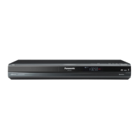
| Type | DVD Recorder |
|---|---|
| Recording Formats | DVD-RAM, DVD-R, DVD-RW, DVD+R, DVD+RW |
| Hard Disk Capacity | 250 GB |
| Progressive Scan | Yes |
| HDMI Output | Yes |
| Component Video Output | Yes |
| Composite Video Output | Yes |
| S-Video Output | Yes |
| Playback Format | DVD-Video, DVD-RAM, DVD-R, DVD-RW, DVD+R, DVD+RW, CD, CD-R, CD-RW |
| Tuner | Analog |
| Video Recording System | MPEG2 |
| Video Output | HDMI, Component, Composite, S-Video |
| Audio Output | Digital Audio (Optical), Analog (RCA) |
| Dimensions | 430 x 79 x 285 mm |
| Digital Audio Output | Optical |