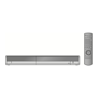
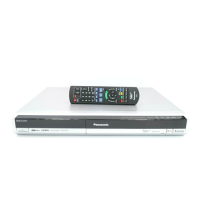
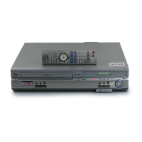
Do you have a question about the Panasonic DMR-EH57EC and is the answer not in the manual?
Basic rules and precautions for servicing the equipment.
Procedures to prevent damage from static electricity to sensitive components.
Safety measures when working with the laser diode to avoid radiation exposure.
Guidelines and cautions related to legal restrictions for service, including lead-free solder.
Overview of the service manual's technical information and ordering procedures.
Warnings and procedures regarding DivX content registration after part replacement.
Instructions for forcibly ejecting a disc when the normal method fails.
Information on self-diagnosis functions and special mode settings for service.
A flowchart outlining the procedure for disassembling the unit.
Diagram showing the location of various Printed Circuit Boards within the unit.
Instructions for removing and reassembling the top casing of the unit.
Instructions for removing and reassembling the front panel assembly.
Instructions for replacing the Hard Disk Drive and ATAPI Printed Circuit Board.
Procedures for replacing the RAM/Digital Printed Circuit Board Module.
Instructions for removing and replacing the DV Jack Printed Circuit Board.
Procedures for removing and replacing the rear panel and fan motor assembly.
Instructions for removing and replacing the Power Printed Circuit Board.
Instructions for removing and replacing the HDMI Printed Circuit Board.
Procedures for removing and replacing main, front jack, and front (L) PCBs.
Describes specific service positions and procedures for checking/repairing components.
Important considerations and procedures when replacing unit components.
Criteria and procedures for verifying normal operation after repairs.
Illustrates the power supply circuit's functional blocks and connections.
Shows the functional blocks and signal flow for analog video processing.
Illustrates the functional blocks and signal paths for analog audio processing.
Depicts the functional blocks and operation of the analog timer system.
Shows the functional blocks and data flow for the HDMI interface.
Shows the overall interconnection between different PCBS and components.
Detailed schematic of the power supply unit's circuitry.
Schematic detailing the first part of the main net section on the main PCB.
Schematic detailing the second part of the main net section on the main PCB.
Schematic detailing the third part of the main net section on the main PCB.
Schematic detailing the fourth part of the main net section on the main PCB.
Schematic for the first part of the AV I/O section on the main PCB.
Schematic for the second part of the AV I/O section on the main PCB.
Schematic for the third part of the AV I/O section on the main PCB.
Schematic for the fourth part of the AV I/O section on the main PCB.
Schematic for the tuner section on the main PCB.
Schematic for the first part of the timer section on the main PCB.
Schematic for the second part of the timer section on the main PCB.
Schematic for the third part of the timer section on the main PCB.
Schematic for the fourth part of the timer section on the main PCB.
Detailed schematic diagram of the HDMI interface circuitry.
Schematic diagram for the DV jack connections and circuitry.
Schematic diagram for the front panel audio/video jack connections.
Schematic diagram for the front left panel circuitry and controls.
Schematic diagram for the ATAPI interface connections.
Illustrations showing the layout of the power and DV jack PCBs.
Illustrations showing the layout of the main printed circuit board (multiple sections).
Illustrations showing the layout of the HDMI printed circuit board.
Illustrations showing the layout of the front jack and front (L) PCBs.
Illustration showing the layout of the ATAPI printed circuit board.
Tables listing voltage measurements and waveform characteristics for various components.
Diagrams illustrating the assembly and parts of the unit.
A comprehensive list of all replaceable parts with their part numbers and descriptions.
| Brand | Panasonic |
|---|---|
| Model | DMR-EH57EC |
| Category | DVD Recorder |
| Language | English |
