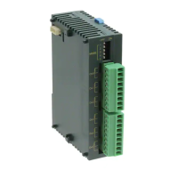
FP2 Serial Data Unit
Sample Programs
8 − 6
8.1 Sample Programs
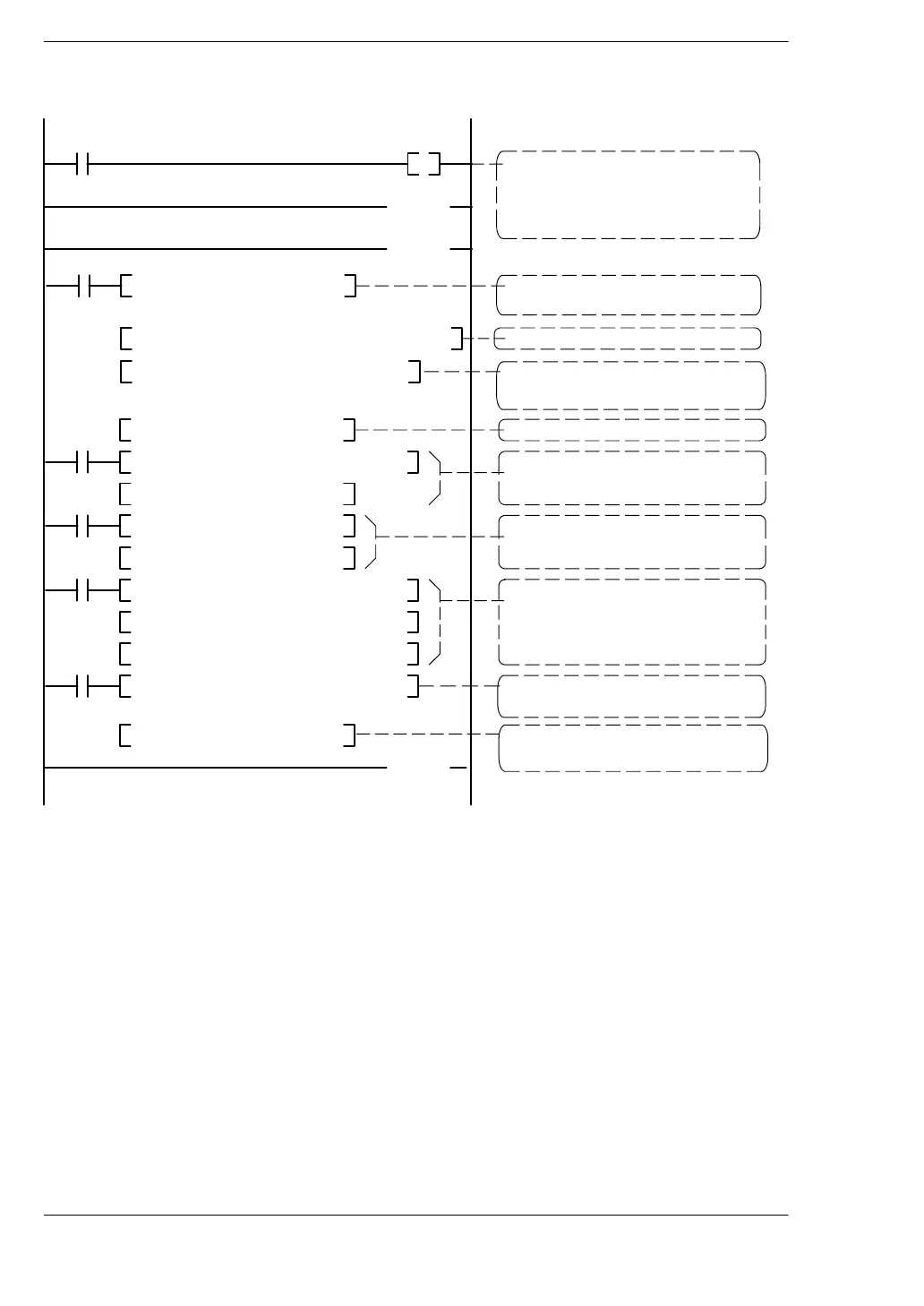
X1 Y11
(ED )
,DT0 ,I0
F0 MV
R9010
, K 2 , I0DT 0
F70 BCC
,DT1 ,DT10
,DT10 ,K1
F71 HEXA
,DT12
,HD
, DT13
F0 MV
,DT1 ,K2
F32 %
,DT2
R9010
, DT90015 , K 1
F60 CMP
,DT12
,DT13
F113 WBSL
R900B
, DT 12 , DT 13
F113 WBSL
,DT2 ,DT0
F22 +
,I0
R9010
, I0DT 0
,DT12
F66 WOR
, I0DT 0
, I0DT 1 , DT 13
F66 WOR
, I0DT 1
,DT2 ,K2
F22 +
,I1
R9010
,DT0 ,I0
F0 MV
(SUB 0)
( RET )
When reception and reading of the
data have been completed, Y11
goes on, and the received buffer is
cleared.
The command store address is
stored in I0.
The BCC is calculated.
The BCC is converted to an ASCII
code.
A CR is added.
The number of data bytes is judged
to be even or odd.
If odd, the data is shifted one byte
to the left.
The BCC and CR are merged.
The number of command words is
set.
The address in which the command
is to be stored is set.