Pin
No.
Mark I/O Function
80 SPMWE O SPM take in test signal output
terminal
Pin
No.
Mark I/O Function
1 DO1 I/O DRAM data 1 in/output terminal
2 DO2 I/O DRAM data 2 in/output terminal
3 WE I DRAM light enable input terminal
4 RAS I DRAM low address strobe input
terminal
5 A9 I DRAM address 9 input terminal
9 A0 I DRAM address 0 input terminal
10
~12
A1
~A3
I DRAM address 1~3 input terminal
13 VCC I Power supply terminal
Pin
No.
Mark I/O Function
1 PDE I Tracking signal input terminal 1 (E ch)
2 PDF I Tracking signal input termianl 2 (F ch)
3 VCC I Power supply connection
4 PDA I Focus signal input termianl 1 (A ch)
5 PDB I Focus signal input terminal 2 (B ch)
6 LPD I Laser PD connection
7 LD O Laser power auto control output
8 RF O RF signal output
9 RFIN I RF signal input
10 CSBRT I Capacitor for detection connection
11 CEA I Capacitor connection for HPF
amplifier
12 BDO O BDO output (“H” : drop out)
13 LDON I LD APC input (“H” : ON, “L” : OFF)
14 GND — Ground connection
15 /RFDET O NRFDET output (“L” : detection)
Pin
No.
Mark I/O Function
1 BCLK O Bit Clock Output for Serial Data
2 LRCK O L/P Clock Signal Output
3 SRDATA O Serial Data Output
4 DVDD1 I Power Supply Input (for Digital
Circuit)
5 DVSS1 I Ground (for Digital Circuit)
6 TX O Digital Audio Interface Signal
Output
(Latches Data at first
Transistion)
7 MCLK I Microprocessor Command
Clock Signal Input
8 MDATA I Microprocessor Command Data
Signal Input
9 MLD I Microprocessor Command Load
Signal Input
10 SENSE I Sense Signal Output (OFT,
FESL, MAGEND, NAJEND,
POSAD, SFG)
(Not Used, Open)
11 /FLOCK O Focus Servo Feeding Signal
Output
(“L”: Feed)
12 /TLOCK O Tracking Servo Feeding Signal
Output
(“L”:Feed)
Pin
No.
Mark I/O Function
14
~18
A4
~A8
I DRAM address 4~8 input terminal
22 OE I DRAM output enable input terminal
(Not used, connected to GND)
23 CAS I DRAM calam address strobe input
terminal
24 DO3 I/O DRAM data 3 in/output terminal
25 DO4 I/O DRAM data 4 in/output terminal
26 VSS — GND terminal
Pin
No.
Mark I/O Function
16 CROSS O CROSS output (Track cross signal
output
17 OFTR O Off-track output (“L” : ON track, “H” :
OFF track)
18 VDET O VDET output (“H” : Vibration detected)
19 ENV O RF envelope detection
20 EMOFF I Not used, connected to power supply
21 TEBPF I Cscillation detect signal input
22 TEN I Tracking error signal input
23 TEOUT O Tracking error signal output
24 FEOUT O Focus error signal output
25 FEN I Focus error signal input
26 VREF O Reference voltage output
27 TBAL I Tracking balance signal input
28 FBAL I Focus balance signal input
Pin
No.
Mark I/O Function
13 BLKCK O Sub-Code Block Clocl Signal
Output
(fBLKCK = 75Hz during Normal
Playback)
14 SQCK I External Clock Signal Input for
Sub-Code Q Resistor)
15 SUBQ O Sub-Code Q Code Output
16 DMUTE I Muting Input (“H”: Mute)
17 STAT O Status Signal Output
(CRC, CUE, CLVS, TTSTVP,
FCLV, SQCK)
18 /RST I Reset Signal Input
19 SMCK O 1/2 - Divided Clock Signal of
Crystal Oscillating at MSEL=
“H” (fSMCK=8.4672 MHz)
1/4 - Divided Clock Signal of
Crystal Oscillating at MSEL= “L”
(fSMCK=4.2336 MHz)
20 CSEL I Frequency Selection Terminal
H= 33.8688 MHz; L= 16.9344
MHz
21 TRV O Traverse Forced Feed Output
22 TVD O Traverse Drive Output
23 PC O Traverse (Spindle) Motor ON
Signal Output (“L”:ON)
12.5. IC72 (MNV4400-T8T) : 4M DRAM
12.6. IC701 (AN8837SBE1) Servo Amplifier
12.7. IC702 (MN662790RSC) Servo Processor / Digital Signal Processor /
Digital Filter / D/A Converter
29
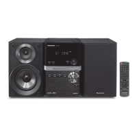
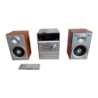
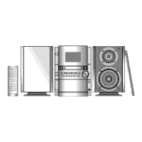
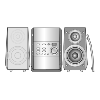
SA-PM30MD