EasyManua.ls Logo

Panasonic SA-VK31 Service Manual

Panasonic SA-VK31
116 pages
To Next Page IconTo Next Page
Page #1 background imageLoading...
Page #1 background image
n AMPLIFIER SECTION
PMPO 2500 W
RMS power output
THD 10% both channels driven
1 kHz (Low channel) 75 W per channel (6 )
10kHz (High channel) 75 W per channel (6 )
Total Bi-Amp power 150 W per channel
A
UX
Input sensitivity 250 mV
Input Impedance 13.3 k
Phone jack
Terminal Stereo, 3.5 mm jack
MIC jack
Sensitivity 0.7 mV, 680
Terminal Mono, 3.5 mm jack (2 system)
n FM TUNER SECTION
Frequency range 87.50 - 108.00 MHz (50 kHz steps)
Sensitivity 2.5µV (IHF)
S/N 26 dB 2.2 µV
A
ntenna terminal(s) 75 (unbalanced)
n AM TUNER SECTION
Frequency range 522 - 1629 kHz (9 kHz steps)
520 - 1630 kHz (10 kHz steps)
Sensitivity
© 2004 Panasonic AVC Networks Singapore Pte.
Ltd. (RCB registration number: 197701580H) All
rights reserved. Unauthorized copying and
distribution is a violation of law.
SA-VK31GC
SA-VK31GS
Colour
(S)... Silver Type
S/N 20 dB (at 999 kHz) 560 µV/m
n CASSETTE DECK SECTION
Track system 4 track, 2 channel
Heads
Record/playback Solid permalloy head
Erasure Double gap ferrite head
Motor DC servo motor
Recording system AC bias 100 kHz
Erasing system AC erase 100 kHz
Tape speed 4.8 cm/s
Overall frequency response (+3 dB, -6 dB at DECK OUT)
NORMAL (TYPE I) 35 Hz - 14 kHz
S/N 50 dB (A weighted)
Wow and flutter 0.18 % (WRMS)
Fast forward and rewind time Approx. 120 seconds with
C-60 cassette tape
n CD SECTION
Discs played [8 cm or 12 cm]
(1) CD- Audio (CD-DA)
(2) Video CD
(3) CD-R/RW (CD-DA, MP3 disc)
(4) MP3
Sampling frequency 44.1 kHz
Decoding 16 bit linear
CD Stereo System
Specifications
ORDER NO. MD0405174C3

Table of Contents

Question and Answer IconNeed help?

Do you have a question about the Panasonic SA-VK31 and is the answer not in the manual?

Panasonic SA-VK31 Specifications

General IconGeneral
BrandPanasonic
ModelSA-VK31
CategoryStereo System
LanguageEnglish

Summary

Safety precautions (for GS only)

Prevention of Electro Static Discharge (ESD) to Electrostatically Sensitive (ES) Devices

Handling Precautions For Traverse Deck

Precaution of Laser Diode

Operation Checks and Main Component Replacement Procedures

Service Position

Description of Error Code

Abnormality Detection for DECK Mechanism

Details error codes related to abnormalities in the deck mechanism.

Abnormality detection for CD/Changer Block

Lists error codes for CD and changer block abnormalities.

Power Supply Related Error Detection

Covers error codes associated with power supply issues.

Self-Diagnostic Function

CD Test Mode Function

Measurements and Adjustments

Schematic Diagram

(A) CD Servo Circuit

Detailed schematic of the CD servo control circuit.

(B) Tuner/Main Circuit

Schematic for the tuner and main control circuitry.

(B) Main Circuit

Schematic diagram illustrating the main circuit board components.

(E) Deck Circuit & (F) Deck Mechanism Circuit

Schematics for the deck circuit and mechanism components.

(G) Power Circuit

Schematic diagram of the power supply and distribution circuits.

(M) VCD Module Circuit

Schematic diagrams for the VCD module circuitry.

Printed Circuit Board

(A) CD Servo P.C.B. (Side A & B)

Layout diagram of the CD servo circuit board (both sides).

(B) Main P.C.B.

Component layout for the main circuit board.

(E) Deck P.C.B. & (F) Deck Mechanism P.C.B.

PCB layout diagrams for the deck circuit and mechanism.

(G) Power P.C.B.

Component layout for the power circuit board.

(H) Transformer P.C.B. & (I) Voltage Selector P.C.B.

PCB layout diagrams for transformer and voltage selector boards.

(J) CD Detect P.C.B., (K) Spindle Position P.C.B., (L) CD Loading P.C.B. & (N) Tuner Pack P.C.B.

PCB layout diagrams for CD detect, spindle, loading, and tuner pack boards.

(M) VCD P.C.B. (Side A & B)

Layout diagrams for the VCD circuit board (both sides).
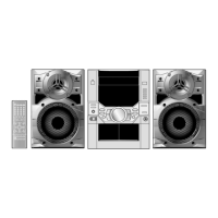
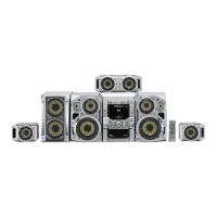
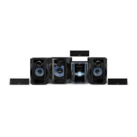
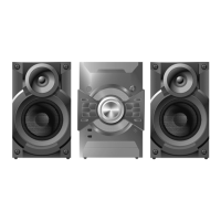
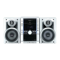
Wiring Connection Diagram

Terminal Function of IC’s

Troubleshooting Guide

Parts Location and Replacement Parts List

Related product manuals