1: Introduction to the BASIC Stamps
BASIC Stamp Programming Manual 2.0c • www.parallaxinc.com • Page 15
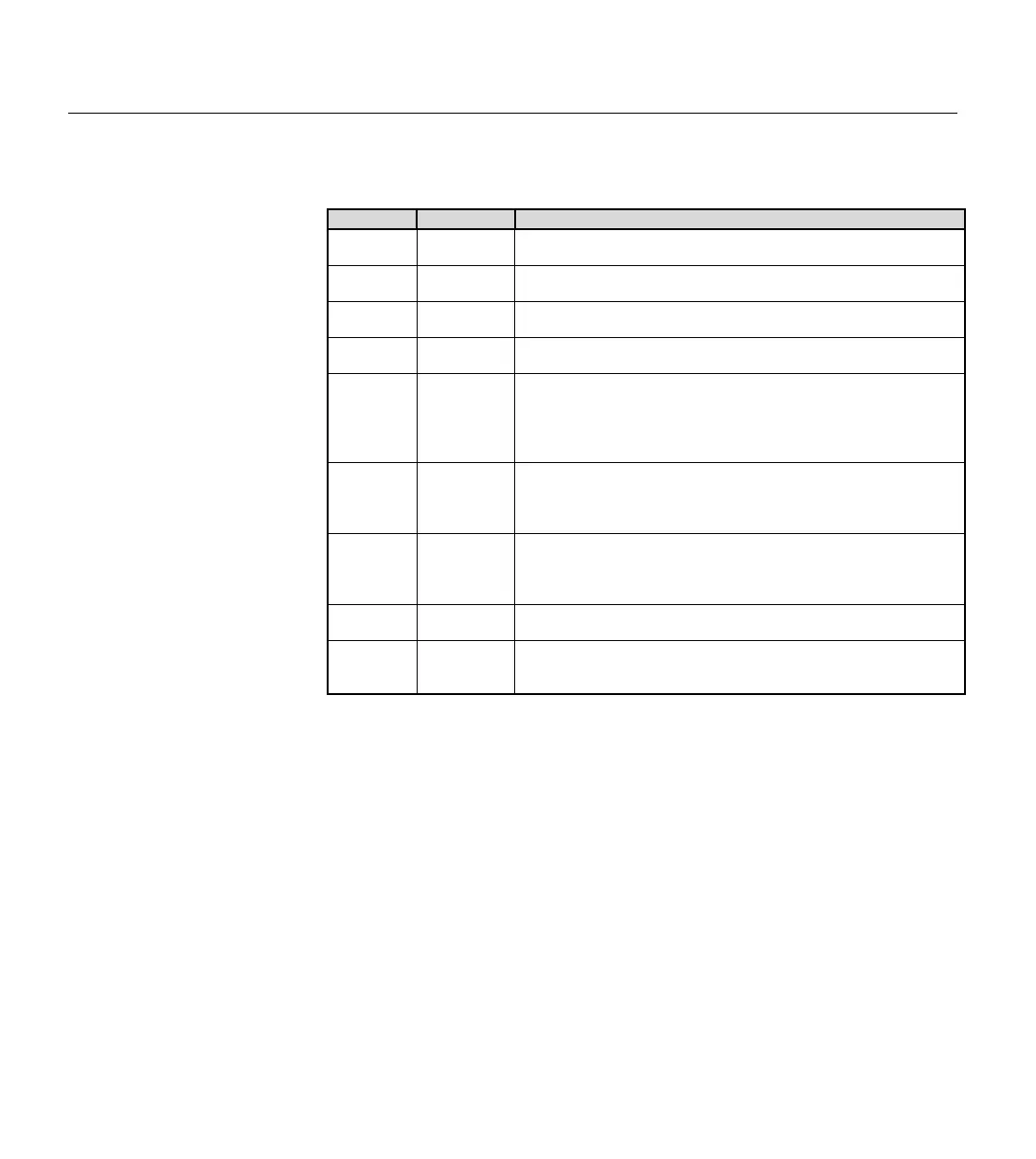
Pin Name Description
1 SOUT
Serial Out: connects to PC serial port RX pin (DB9 pin 2 / DB25
pin 3) for programming.
2 SIN
Serial In: connects to PC serial port TX pin (DB9 pin 3 / DB25 pin
2) for programming.
3 ATN
Attention: connects to PC serial port DTR pin (DB9 pin 4 / DB25
pin 20) for programming.
4 VSS
System ground: (same as pin 23) connects t
pin (DB9 pin 5 / DB25 pin 7) for programming.
5-20 P0-P15
General-purpose I/O pins: each can source and sink 30 mA.
However, the t
otal of all pins should not exceed 75 mA (source or
sink) if using the internal 5-volt regulator. The total per 8-pin
groups (P0 – P7 or P8 – 15) should not exceed 100 mA (source
or sink) if using an external 5-volt regulator.
21 VDD
5-volt DC input/output: if an unregulated voltage is applied to the
VIN pin, then this pin will output 5 volts. If no voltage is applied to
the VIN pin, then a regulated voltage between 4.5V and 5.5V
should be applied to this pin.
22 RES
Reset input/output: goes low when power supply is less than
approximately 4.2 volts, causing the BASIC Stamp to reset. Can
be driven low to force a reset. This pin is internally pulled high
and may be left disconnected if not needed. Do not drive high.
23 VSS
System ground: (same as pin 4) connects to power supply’s
ground (GND) terminal.
24 VIN
Unregulated power in: accepts 5.5 - 12 VDC (7.5 recommended),
which is then internally regulated to 5 volts. May be left
unconnected if 5 volts is applied to the VDD (+5V) pin.
See the "BASIC Stamp Programming Connections" section, below, for
more information on the required programming connections between the
PC and the BASIC Stamp.
Table 1.4: BASIC Stamp 2sx Pin
Descriptions.