Introduction to the BASIC Stamps
Page 18 • BASIC Stamp Programming Manual 2.0b • www.parallaxinc.com
Development Boards
We provide a number of development boards to make using the BASIC
Stamps more convenient. Below is a short description of the boards and
their intended use. Please refer to the development board’s
documentation (if any) for more details.
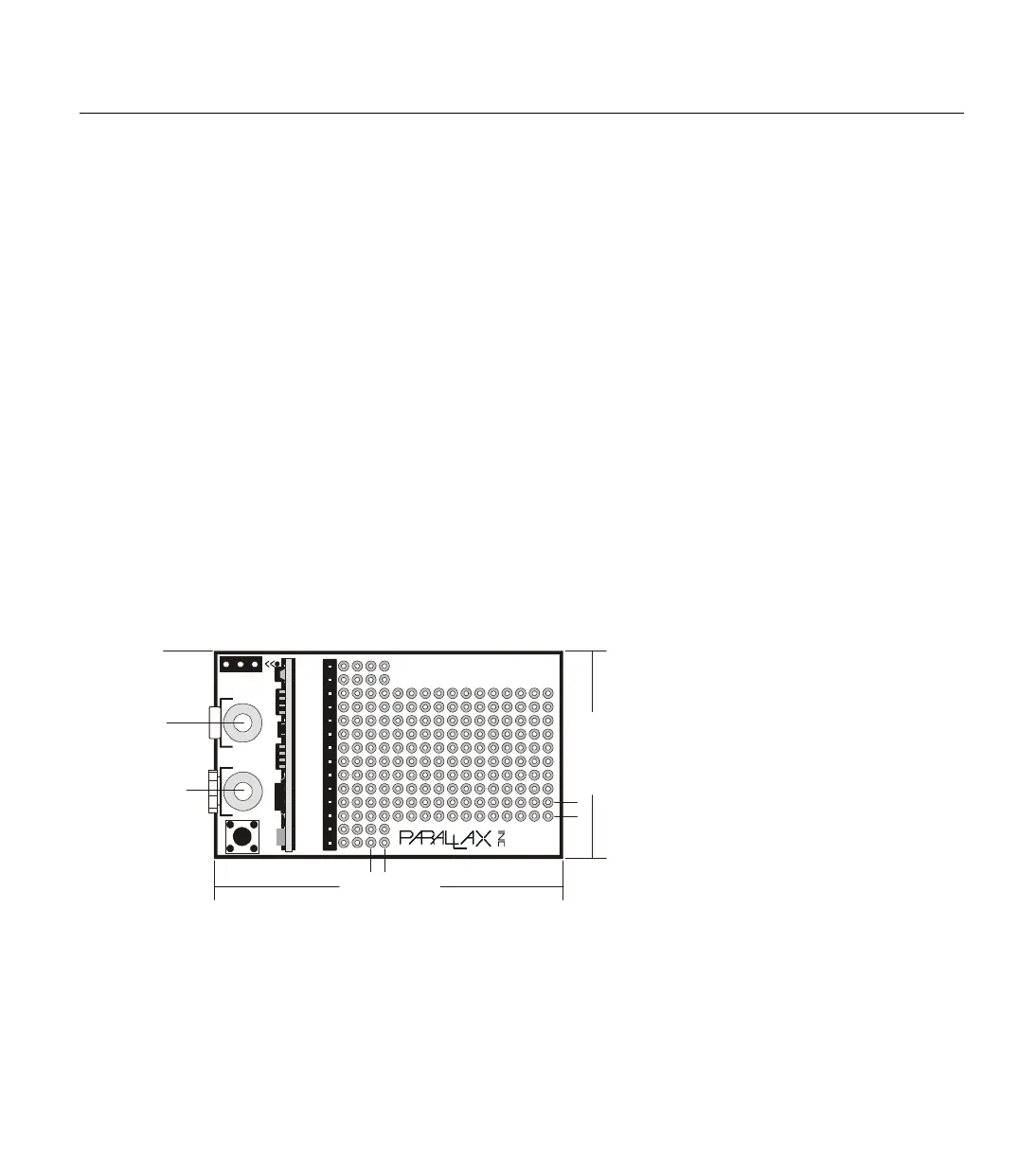
BASIC Stamp 1 Carrier Board (Rev. E)
The BASIC Stamp 1 Carrier Board (also called the BS1 Carrier Board) is
designed to accommodate the BS1-IC module. The BASIC Stamp 1 Carrier
Board provides nearly the same form factor and prototyping space as with
the BASIC Stamp 1 Rev. D, but with the added feature of the reset button.
Figure 1.12 shows the BASIC Stamp 1 Carrier Board with the BS1-IC
properly inserted into the socket. This board features a 3-pin
programming header and 9-volt battery clips to connect a power source.
A male, 14-pin 0.1” header (to the left of the through-hole array) allows
access to all the BS1’s pins. The first two columns of solder pads (closest to
the header) are connected to the respective header pin. All other solder
pads are isolated from each other. The entire through-hole array is
provided for permanent or semi-permanent circuit design.
Figure 1.12: BASIC Stamp 1
Carrier Board (Rev. E) (shown with
BS1-IC properly inserted) (27110)
©1994
REV E
TM
Vin
Vss
PCO
PCI
Vdd
RES
P0
P1
P2
P3
P4
P5
P6
P7
BASIC Stamp
ΤΜ
.1“ (2.54 mm)
.1“ (2.54 mm)
1.5“ (38 mm)
2.5“ (63.5 mm)
.5“ (13 mm)
.5“ (13 mm)
Reset
BS1-IC
2 11 15
PC Parallel Port