Introduction to the BASIC Stamps
Page 20 • BASIC Stamp Programming Manual 2.0b • www.parallaxinc.com
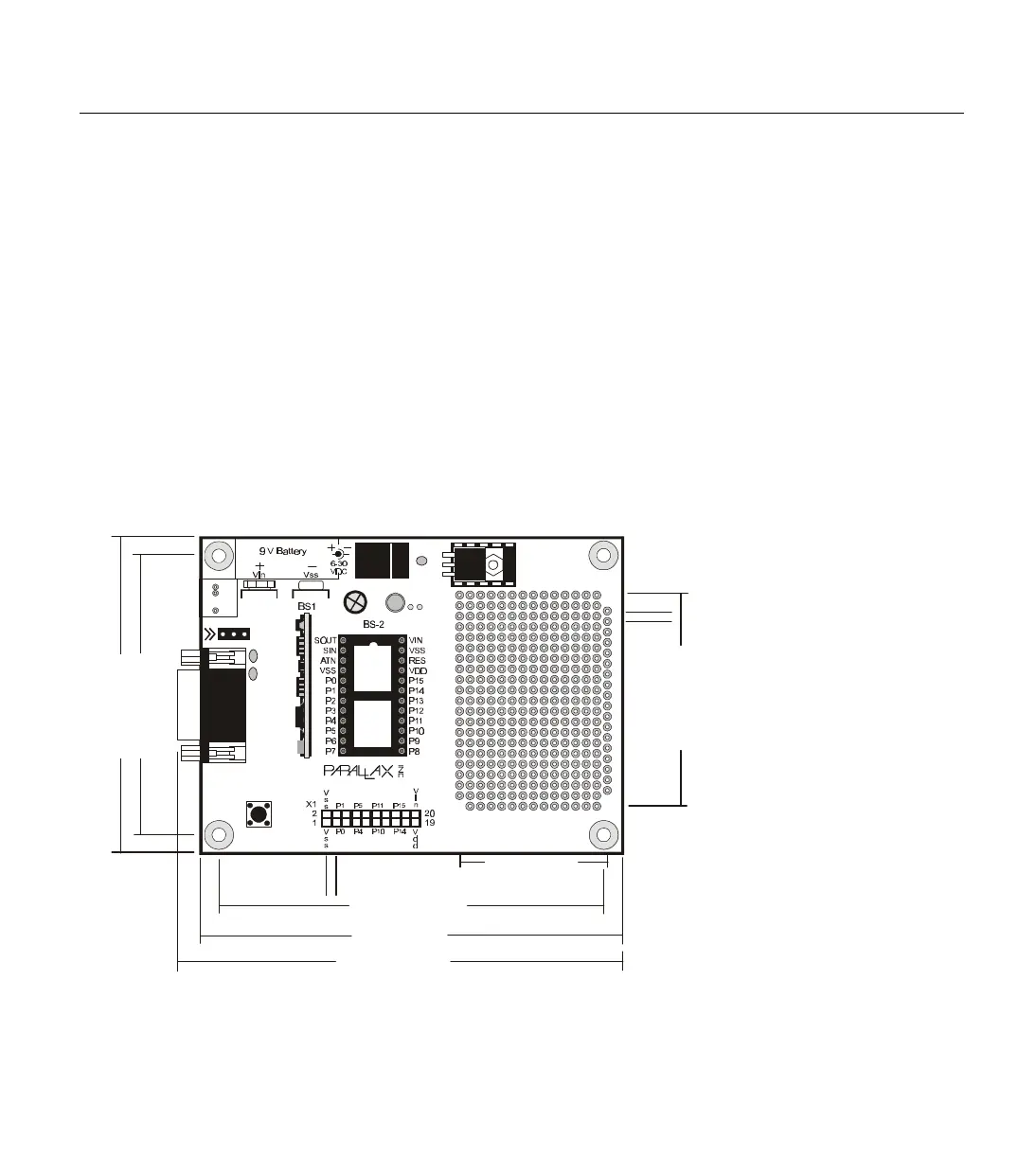
BASIC Stamp Super Carrier (Rev. A)
The BASIC Stamp Super Carrier board is designed to accommodate the
BS1-IC, BS2-IC, BS2e-IC and BS2sx-IC modules. This board provides
ample prototyping space for simple or moderate circuits. Figures 1.14 and
1.15 show the board with the BS1-IC or BS2-IC properly inserted into the
sockets. NOTE: Do not power-up the board with a BS1-IC and a BS2-IC,
BS2e-IC or BS2sx-IC inserted at the same time. This board features a 3-
pin programming connector (Stamp 1), DB9 programming connector
(Stamp 2, 2e, 2sx), reset button, 9-volt battery clips, barrel connector,
separate 5-volt regulator, and power LED. A female, 20-pin 0.1” socket
allows access to all the module’s pins. Many of the solder pads (see Figure
1.16) are connected to each other in a fashion that allows breadboard-like
assembly of circuits (examine the through-hole array carefully before
soldering). Note: the barrel jack is designed for a center positive, 2.1 mm
(pin) x 5.5 mm (barrel) plug.
Figure 1.14: BASIC Stamp Super
Carrier Board (Rev. A) (shown with
BS1-IC properly inserted) (27130)
Reset
Pwr
Need Tech Support?
Send email to:
stamptech@parallaxinc.com
Basic Stamp Super Carrier
www.parallaxinc.com (916) 624-8333 ©1999
J3
TM
C2
+
Rev A
C3
J1
C4
P15
P14
P13
P12
P11
P10
P9
P8
P7
P6
P5
P4
P3
P2
P1
P0
Vdd
Vdd
Vss
Vss
Vss
C1
Vin
Vss
PCO
PCI
Vdd
Rst
P0
P1
P2
P3
P4
P5
P6
P7
Vin
J2
Vss
Rocklin, CA - USA
4” (102mm)
4.25” (107mm)
3.25” (94mm)
1.4” (36mm)
0
.
1
”
(
3
m
m
)
3.1” (78mm)
2.7” (70mm)
2.0” (51mm)
0
.
1
”
(
3
m
m
)