SHIFTOUT - BASIC Stamp Command Reference
Page 314 • BASIC Stamp Programming Manual 2.0b • www.parallaxinc.com
At their heart, synchronous-serial devices are essentially shift-registers;
trains of flip-flops that receive data bits in a bucket brigade fashion from a
single data input pin. Another bit is input each time the appropriate edge
(rising or falling, depending on the device) appears on the clock line.
The SHIFTOUT instruction first causes the clock pin to output low and the
data pin to switch to output mode. Then, SHIFTOUT sets the data pin to
the next bit state to be output and generates a clock pulse. SHIFTOUT
continues to generate clock pulses and places the next data bit on the data
pin for as many data bits as are required for transmission.
Making SHIFTOUT work with a particular device is a matter of matching
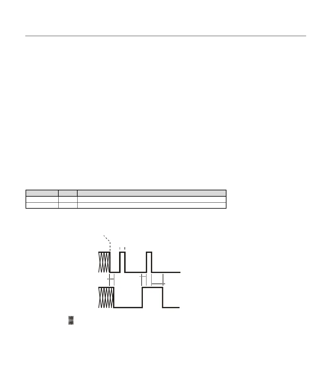
the mode and number of bits to that device’s protocol. Most
manufacturers use a timing diagram to illustrate the relationship of clock
and data. One of the most important items to look for is which bit of the
data should be transmitted first; most significant bit (MSB) or least
significant bit (LSB). Table 5.92 shows the values and symbols available
for the Mode argument and Figure 5.39 shows SHIFTOUT’s timing.
Symbol Value Meaning
LSBFIRST 0
-first
MSBFIRST 1
-first
(Msb is most-significant bit; the highest or leftmost bit of a nibble, byte, or word. Lsb is the
least-significant bit; the lowest or rightmost bit of a nibble, byte, or word.)
Figure 5.39: SHIFTOUT Timing
Diagram. Refer to the SHIFTOUT
Quick Answers table for timing
information on t
h
l
a
and t
b
.
Table 5.92: SHIFTOUT Mode
SHIFTOUT OPERATION.
t
h
Clock
(cpin)
Data
(dpin)
t
l
SHIFTOUT begins,
makes Cpin output low
=previous state of pin unknown
t
a
t
a
t
b