1818
4-2. CIRCUIT BOARDS LOCATION
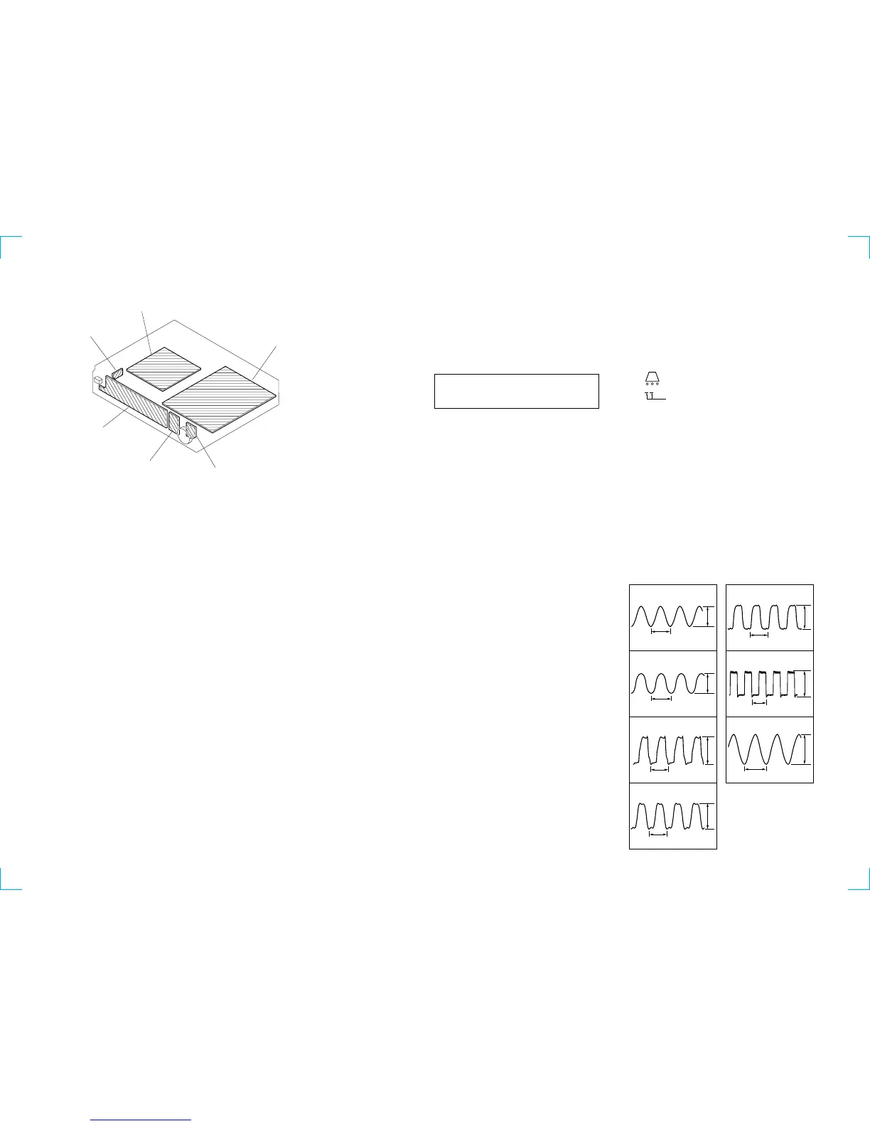
• Waveforms
MAIN board
• U : B+ Line.
• V : B– Line.
• Voltages and waveforms are dc with respect to ground under
no-signal (detuned) conditions.
no mark : FM
( ) : MW
< > : LW
∗
: Impossible to measure
• Voltages are taken with a VOM (Input impedance 10 MΩ).
Voltage variations may be noted due to normal production tol-
erances.
• Waveforms are taken with a oscilloscope.
Voltage variations may be noted due to normal production tol-
erances.
• Circled numbers refer to waveforms.
• Signal path.
F : FM
f : AM
For printed wiring boards.
Note:
• X : parts extracted from the component side.
• b : Pattern from the side which enables seeing.
Note:
The components identified by mark 0 or dotted line with
mark 0 are critical for safety.
Replace only with part number specified.
• Indication of transistor
C
These are omitted
EB
THIS NOTE IS COMMON FOR PRINTED WIRING
BOARDS AND SCHEMATIC DIAGRAMS.
(In addition to this, the necessary note is printed in
each block.)
For schematic diagrams.
Note:
• All capacitors are in µF unless otherwise noted. pF: µµF 50 WV
or less are not indicated except for electrolytics and tantalums.
• All resistors are in Ω and
1
/
4
W or less unless otherwise speci-
fied.
•
f
: internal component.
• C : panel designation
AC SW board
KEY SW board
POWER board
DISPLAY board
ENCODER board
MAIN board
1 IC201 wf
4.6Vp-p
222.2ns
2 IC401 qf
2.2Vp-p
230.8ns
3 IC501 rg
3.3Vp-p
40.7ns
4 IC502 qd
6.0Vp-p
20.3ns
5 IC502 ta
5.6Vp-p
40.7ns
6 IC502 tf
6.0Vp-p
162.7ns
7 IC601 yk
3.5Vp-p
100.0ns
 Loading...