IC Data Sheets
EN 53TPM10.1E LA 8.
2014-Jul-18
back to
div.table
8. IC Data Sheets
This chapter shows the internal block diagrams and pin
configurations of ICs that are drawn as “black boxes” in the
electrical diagrams (with the exception of “memory” and “logic”
ICs).
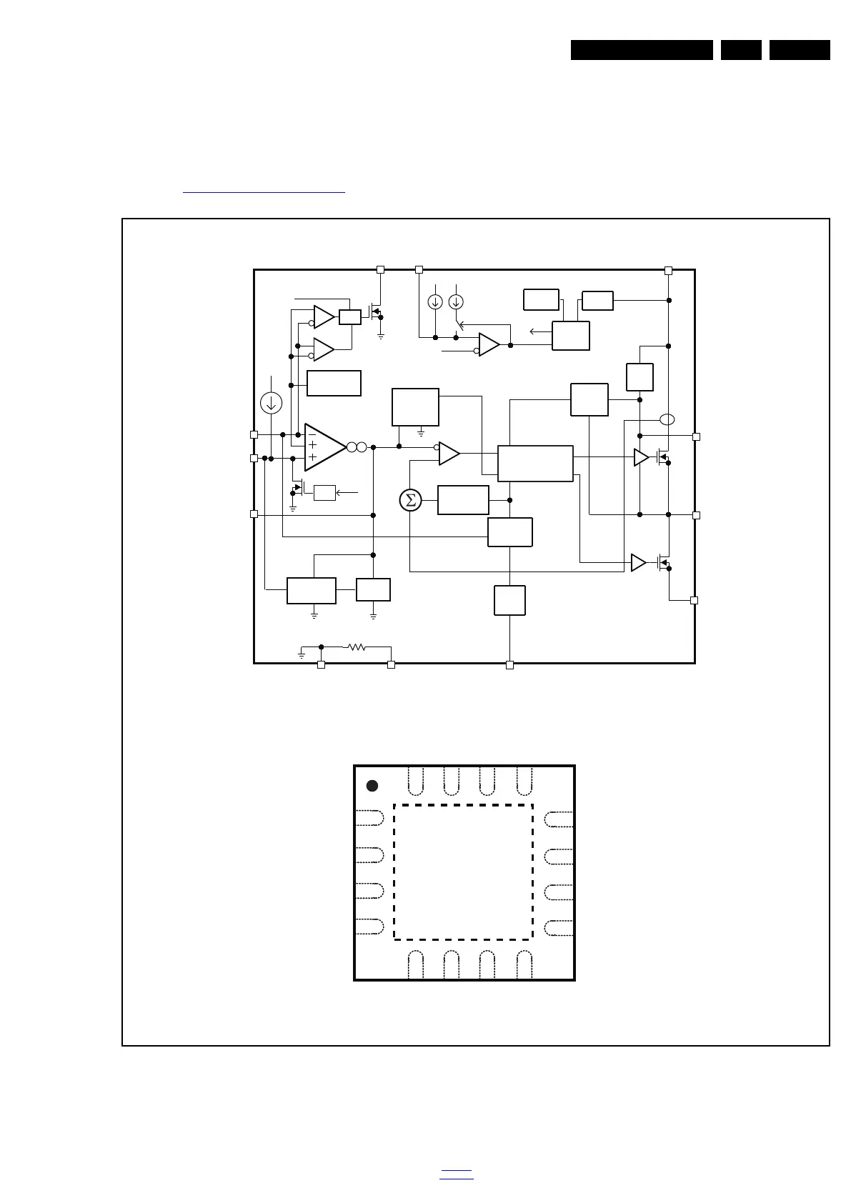
8.1 Diagram 10-10-1 System Power 1, B01,TPS54519RTE (IC U702)
Figure 8-1 Internal block diagram and pin configuration
19430_300_130116.eps
130116
Block diagram
Pinning information
DGRWP
TOOB
PH
TR
NE
DNGA
VIN
ESNESV
PMOC
15 14 13
GND
12
11
10
9
8
765
16
GND
VIN
NIV
PH
PH
1
2
3
4
SS/TR
TPS54519
ERROR
AMPLIFIER
Boot
Charge
Boot
UVLO
UVLO
Current
Sense
Oscillator
Frequency
Shift
Slope
Compensation
PWM
Comparator
Minimum
COMP Clamp
Maximum
Clamp
Vo l t age
Reference
Overload
Recovery
VSENSE
SS/TR
COMP
RT
PH
BOOT
VIN
AGND
Thermal
Shutdown
EN
Enable
Comparator
Shutdown
Logic
Shutdown
Enable
Threshold
Logic
Shutdo
wn
PWRGD
THERMALP
AD
GND
Logic
Shutdown
107%
93%
Logic and PWM
Latch
i
1
i
hys
TPS54519