PDP-503PE, PDP-503PU
90
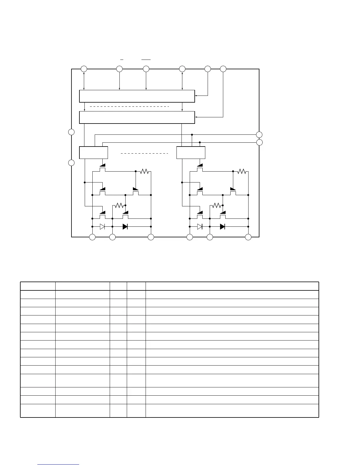
DB
GND
DATA
VDD
GND VH2HVO33 - 64
DAA/B
64 bit Shift Register
64 bit Latch
Selector Selector
CLR CLK LE
OC1
OC2
DATA
GND VH1HVO1 - 32
Name Pin No. I/O Num. Function
CLK 39 I 1 Shift clock (start edge partial response)
DA 44 I/O 1 The serial data input of shifting register
DB 37 I/O 1 The serial data output of shifting register
LE 40 I 1 It output data done a latch of by "L" level
A/B 36 I 1 A shift directional control signal of shift register
CLR 45 I 1 It do data of shift register with "L" by "L" level
OC1 42 I 1 An output control terminal of HVO
OC2 43 I 1 An output control terminal of HVO
HVO 1-30, 51-82, 99, 100 O 64 High voltage drive output (HVO1 - HVO64)
VDD 41 − 1 Logic power supply
GND
34, 35, 38, 46, 47,
87-89, 91-94
− 12 Standard potential. This is common to HVO1 - HVO64.
VH1 84, 85, 49, 50 − 4 The high potential circuit power supply which is common to HVO1 - HVO32
VH2 31, 32, 96, 97 − 4 The high potential circuit power supply which is common to HVO33 - HVO64
NC
33, 48, 95, 83, 86,
90, 98
− 7 It is the insulation electrically
•
Block Diagram
•
Pin Function
 Loading...