NB-IoT Module Series
BC66 Hardware Design
BC66_Hardware_Design 33 / 59
Module
SIM_VDD
SIM_GND
SIM_RST
SIM_CLK
SIM_DATA
22R
22R
22R
100nF
USIM Card Connector
GND
TVS
33pF33pF 33pF
VCC
RST
CLK IO
VPP
GND
GND
33pF
10K
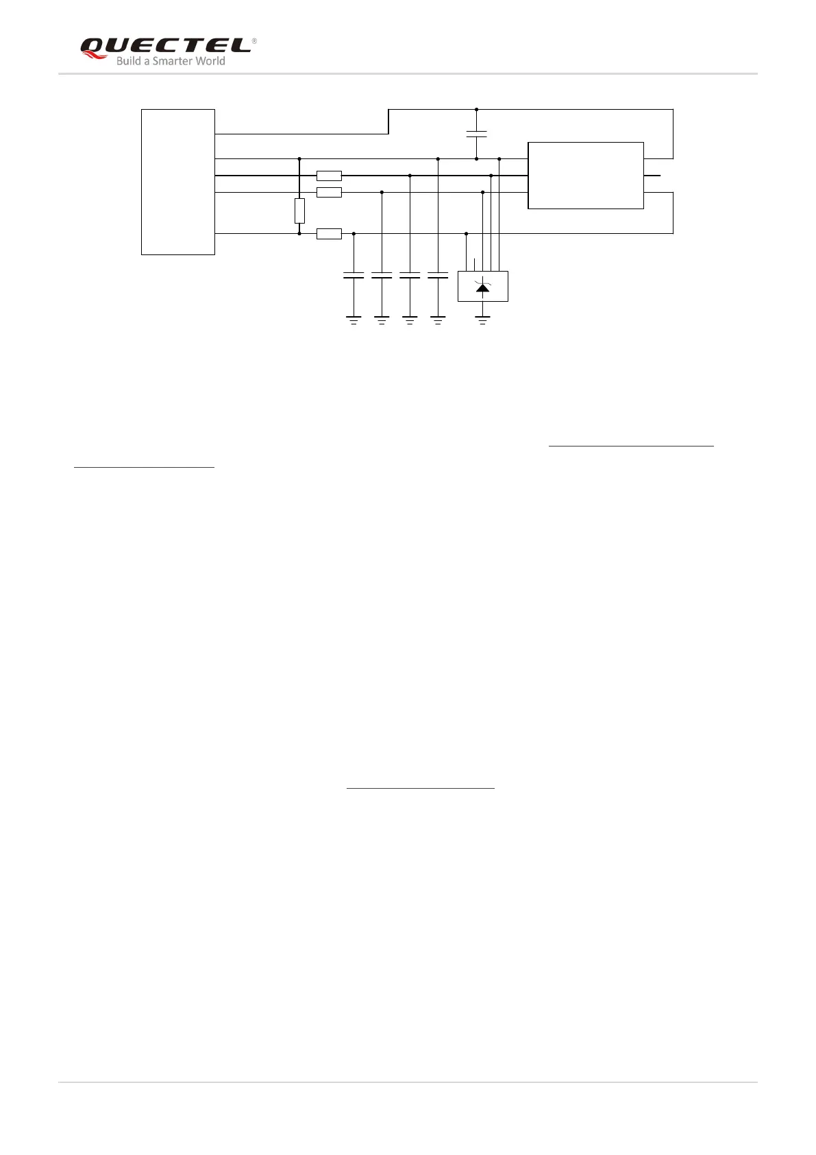
Figure 21: Reference Circuit for USIM Interface with a 6-pin USIM Card Connector
For more information of USIM card connector, please visit http://www.amphenol.com or
http://www.molex.com.
In order to enhance the reliability and availability of USIM card in application, please follow the criteria
below in USIM circuit design:
Keep the placement of USIM card connector as close as possible to the module. Keep the trace
length as less than 200mm as possible.
Keep USIM card signals away from RF and VBAT traces.
Assure the trace between the ground of module and that of USIM card connector is short and wide.
Keep the trace width of ground no less than 0.5mm to maintain the same electric potential. The
decouple capacitor between SIM_VDD and GND should be not more than 1μF and be placed close
to the USIM card connector.
To avoid cross talk between SIM_DATA and SIM_CLK, keep them away from each other and shield
them separately with surrounded ground.
In order to offer good ESD protection, it is recommended to add a TVS diode array. For more
information of TVS diode, please visit http://www.onsemi.com. The ESD protection device should be
placed as close to USIM card connector as possible, and make sure the USIM card signal lines go
through the ESD protection device first and then to the module. The 22Ω resistors should be
connected in series between the module and the USIM card connector so as to suppress EMI
spurious transmission and enhance ESD protection. Please note that the USIM peripheral circuit
should be close to the USIM card connector.
Place the RF bypass capacitors (33pF) close to the USIM card connector on all signal traces to
improve EMI suppression.