NB-IoT Module Series
BC66 Hardware Design
BC66_Hardware_Design 39 / 59
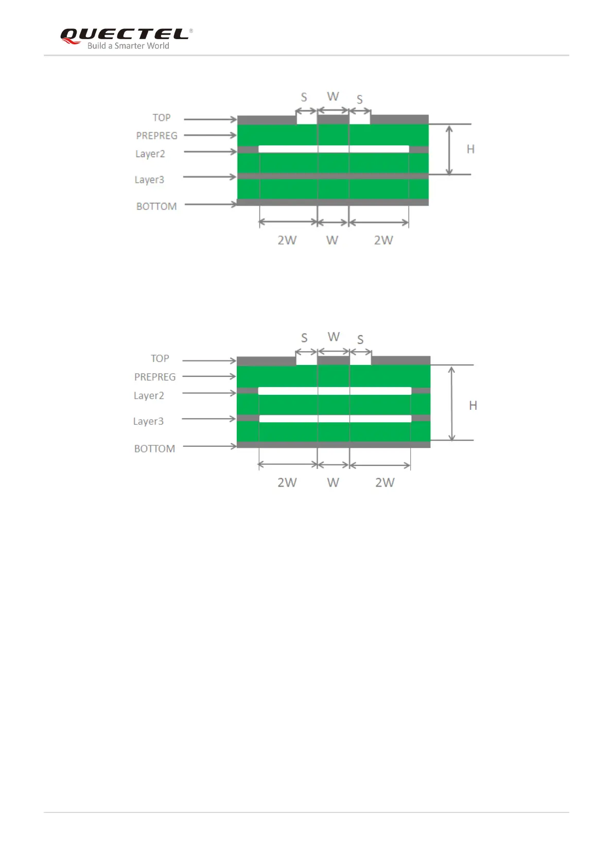
Figure 27: Coplanar Waveguide Design on a 4-layer PCB (Layer 3 as Reference Ground)
Figure 28: Coplanar Waveguide Design on a 4-layer PCB (Layer 4 as Reference Ground)
In order to ensure RF performance and reliability, the following principles should be complied with in RF
layout design:
Use an impedance simulation tool to accurately control the characteristic impedance of RF traces to
50Ω.
The GND pins adjacent to RF pins should not be designed as thermal relief pads, and should be fully
connected to ground.
The distance between the RF pins and the RF connector should be as short as possible, and all the
right-angle traces should be changed to curved ones.
There should be clearance under the signal pin of the antenna connector or solder joint.
The reference ground of RF traces should be complete. Meanwhile, adding some ground vias around
RF traces and the reference ground could help to improve RF performance. The distance between
the ground vias and RF traces should be no less than two times as wide as RF signal traces (2×W).
For more details, please refer to document [2].