LPWA Module Series
BG96 Hardware Design
BG96_Hardware_Design 34 / 79
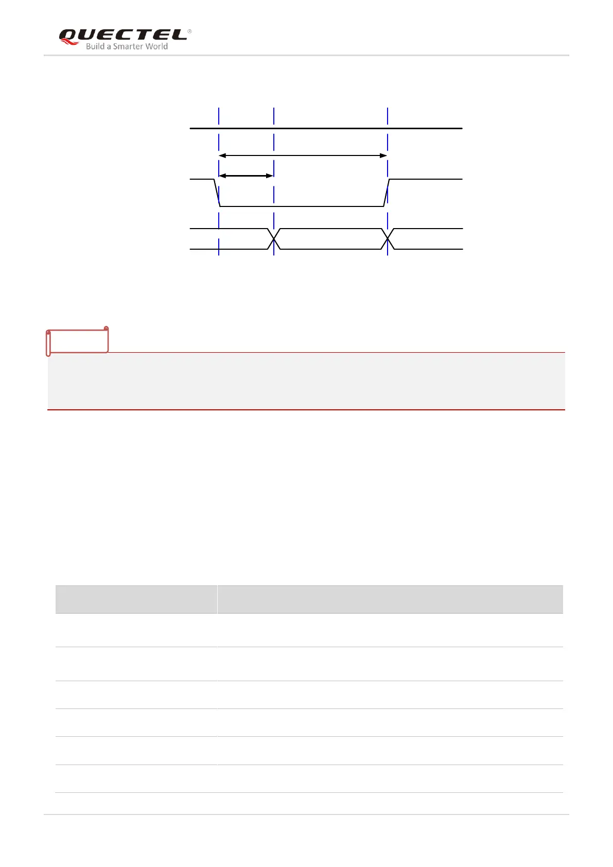
The reset scenario is illustrated in the following figure.
VBAT
≥150ms
Resetting
Module
Status
Running
RESET_N
Restart
≤460ms
V
IL
≤0.5V
Figure 12: Timing of Resetting Module
1. Use RESET_N only when turning off the module by AT+QPOWD command and PWRKEY pin both
failed.
2. Ensure that there is no large capacitance on PWRKEY and RESET_N pins.
3.8. (U)SIM Interface
The (U)SIM interface circuitry meets ETSI and IMT-2000 requirements. Both 1.8V and 3.0V (U)SIM cards
are supported.
Table 9: Pin Definition of (U)SIM Interface
(U)SIM card insertion detection
Power supply for (U)SIM card
Either 1.8V or 3.0V is supported
by the module automatically.
Reset signal of (U)SIM card
Data signal of (U)SIM card
Clock signal of (U)SIM card
Specified ground for (U)SIM card