LTE-A Module Series
EG060V-EA Hardware Design
EG060V-EA_Hardware_Design 45 / 82
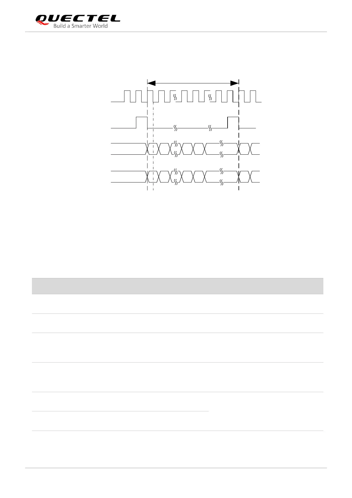
The module supports 16-bit linear data format. The following figures show the relationship between 8 kHz
PCM_SYNC and 2048 kHz PCM_CLK in the primary mode.
PCM_CLK
PCM_SYNC
PCM_DOUT
MSB
LSB
MSB
125 μs
1 2 256255
PCM_DIN
MSB
LSBMSB
Figure 23: Primary Mode Timing
The following table shows the pin definition of PCM and I2C interfaces which can be applied on audio
codec design.
Table 14: Pin Definition of PCM and I2C Interfaces
Clock and mode can be configured by AT command, and the default configuration is master mode using
1.8 V power domain.
If unused, keep it open.
1.8 V power domain.
If unused, keep it open.
1.8 V power domain. In master mode, it
is an output signal. In slave mode, it is
an input signal.
If unused, keep it open.
1.8 V power domain. In master mode, it
is an output signal. In slave mode, it is
an input signal.
If unused, keep it open.
I2C serial clock (or
external codec)
Needs to be pulled up to 1.8 V.
I2C serial data (for
external codec)
 Loading...