Smart Module Series
SG368Z_Series_Hardware_Design 87 / 113
Table 40: Bluetooth Transmitting and Receiving Performance (Unit: dBm)
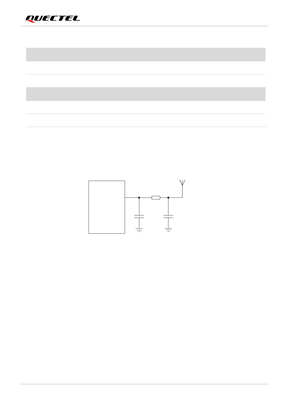
5.1.3. Reference Design
A reference design of Wi-Fi & Bluetooth antenna interface is shown as below. C1 and C2 are not mounted
by default. Only a 0 Ω resistor is mounted on R1.
Figure 30: Reference Design of Wi-Fi & Bluetooth Antenna
5.2. RF Routing Guidelines
When designing PCB, characteristic impedance of all RF traces should be controlled to 50 Ω. Generally,
the impedance of RF traces is determined by materials’ dielectric constant, trace width (W), space
between RF traces and grounds (S) and height from the reference ground to the signal layer (H).
Microstrip or coplanar waveguide is typically used in RF layout to control characteristic impedance. The
following are reference designs of microstrip or coplanar waveguide with different PCB structures when
characteristic impedance of RF traces is controlled to 50 Ω.
 Loading...