156 Rabbit 2000 Microprocessor
Figure 15-3, Figure 15-4, and Figure 15-5 illustrate the memory and I/O read and write cycles.
The Rabbit operates at 2 clocks per bus cycle plus any wait states that might be specified.
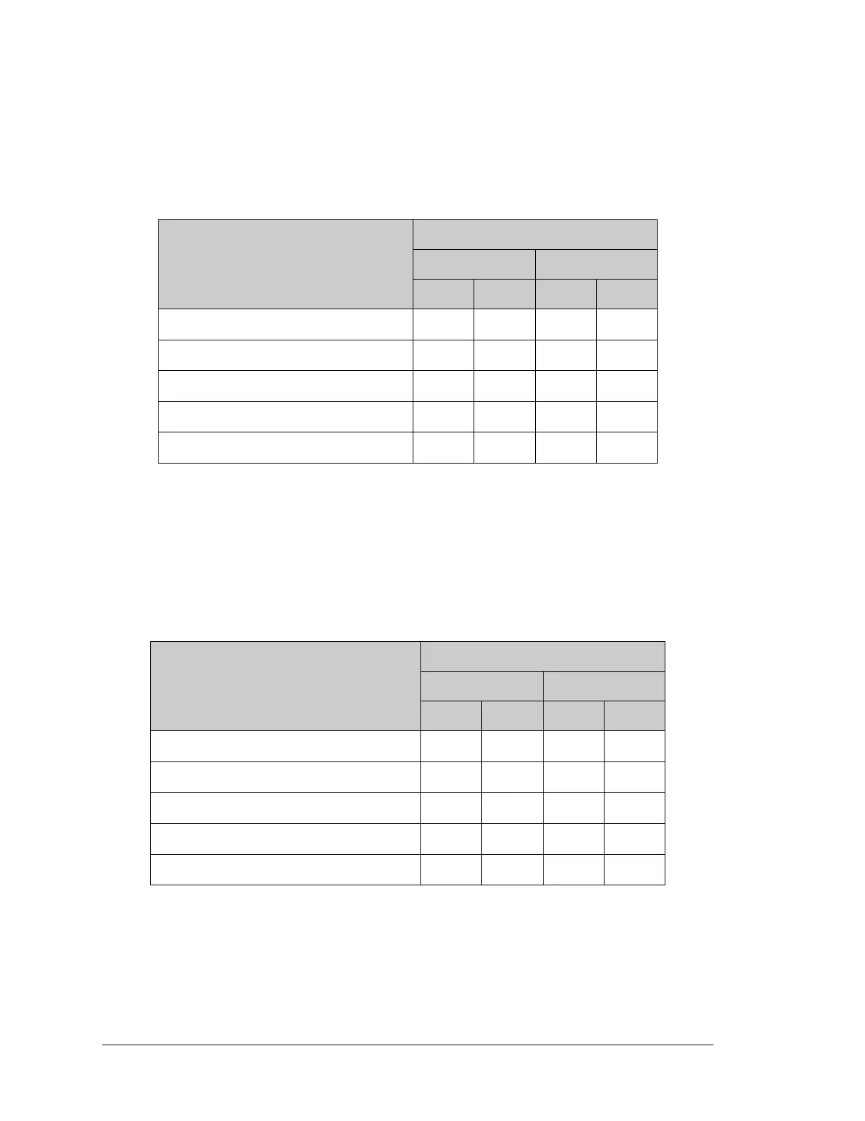
The following memory read time delays were measured.
The measurements were taken at the 50% points under the following conditions.
• T = -40°C to 85°C, V = 5.0 V ±10%
• Internal clock to nonloaded CLK pin delay ≤ 1 ns @ 85°C/4.5 V
The following memory write time delays were measured.
The measurements were taken at the 50% points under the same conditions that the mem-
ory read delays were measured.
Table 15-3. Memory Read Time Delays
Time Delay
Output Capacitance
20 pF 70 pF
min. max. min. max.
Clock to address delay (T
adr
)
— 8 ns — 14 ns
Clock to memory chip select delay (T
CSx
)
— 8 ns — 14 ns
Clock to memory read strobe delay (T
OEx
)
— 6 ns — 12 ns
Data setup time (T
setup
)
3 ns — 3 ns —
Data hold time (T
hold
)
0 ns — 0 ns —
Table 15-4. Memory Write Time Delays
Time Delay
Output Capacitance
20 pF 70 pF
min. max. min. max.
Clock to address delay (T
adr
)
— 8 ns — 14 ns
Clock to memory chip select delay (T
CSx
)
— 8 ns — 14 ns
Clock to memory write strobe delay (T
WEx
)
— 6 ns — 12 ns
High Z to data valid relative to clock (T
DHZV
)
— 11 ns — 17 ns
Data valid to high Z relative to clock (T
DVHZ
)
— 11 ns — 11 ns