divided by
6
divided
by 2
=
887.041 KHz. What
did
change?
Two
signals changed. "LATCH"
is sourced at Z24,
pin 3. In 64 character format,
the latch pulse
was
only
one
clock cycle (Master
Clock) wide, having
a period of 6 clock
cycles. In
32 character mode, the pulsewidth
has doubled
to 2
clock cycles
and its period
is now 12 clock cycles. The
other signal
that changed was C1.
Sourced at
Z43,
pin
7,
it
was
a
square
wave at the same
rate as the chain signal; but
in 32 character
mode, it is held low all
the
time. The signals
that changed are very important
to the video processor
section. The
first,
LATCH,
is used
to delay a character
between RAM
and the character generator. The second
signal,
C1, determines if the RAM
has 1024 or 512 useable
addresses.
Z65
is
a
binary
counter that is
split into
two parts. The
chain
input from the
conditioning logic
is applied
to pin 1
of Z65. The
B and C outputs
are used
for video RAM
addressing,
and the
output of Z65
at pin 8 is applied
to the
next counter
in the chain.
This
part of
Z65
divides the
chain frequency
by 4. Since
the chain
is
887.0461 KHz,
the output
of
Z65,
pin
8,
is
221.760 KHz. The
other part
of
Z65
will
be used later.
The
next counter in
the chain is Z50.
The input
is on pin
14 and
the divided frequency
is at pin
11. This device is
externally
modified
to divide the input
frequency
by 14.
Z50
counts
up normally
to a binary value
of 13. Hence the
counter's
outputs
are as follows:
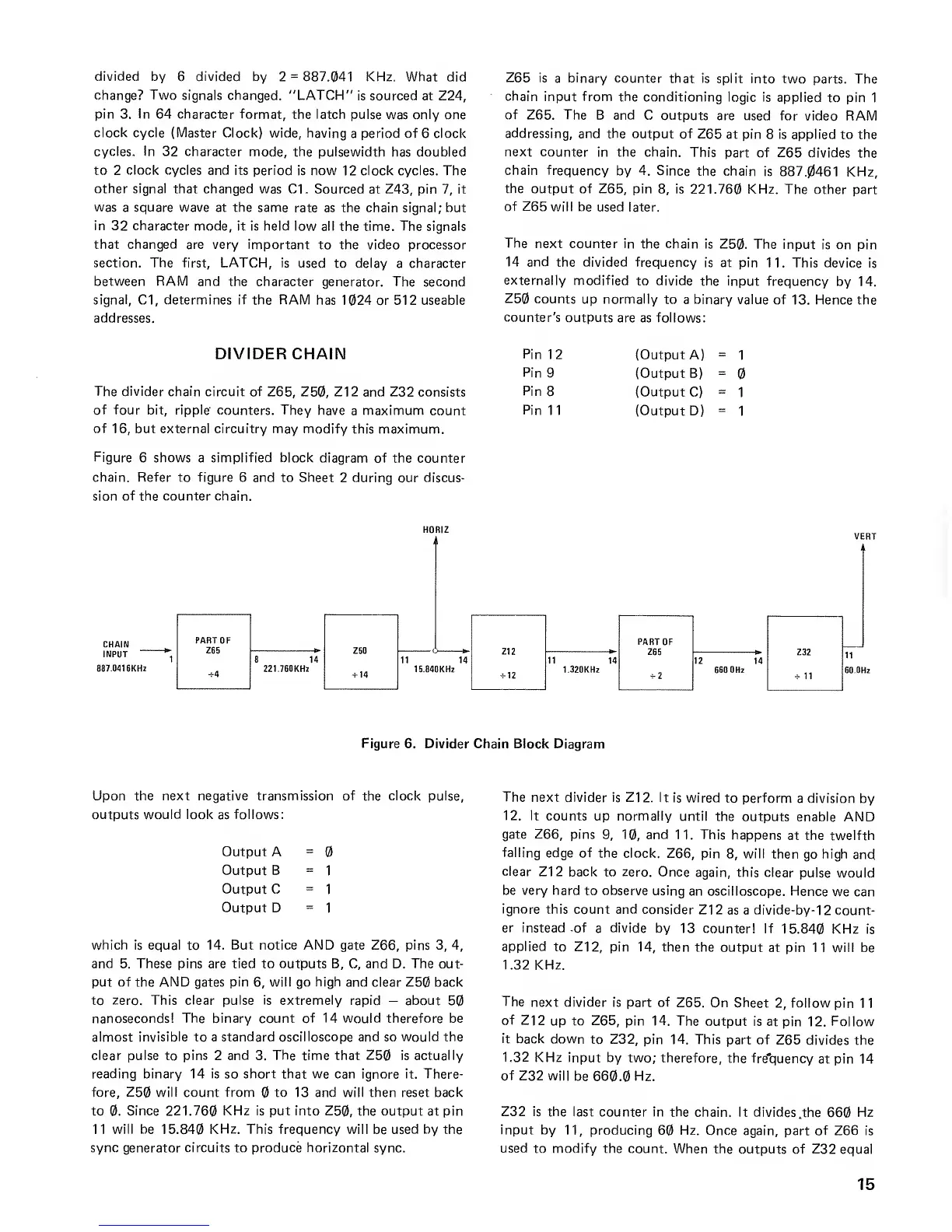
DIVIDER
CHAIN
The divider chain
circuit of Z65, Z50, Z12
and
Z32
consists
of four bit, ripple counters. They
have
a
maximum
count
of
16,
but external circuitry may modify
this maximum.
Figure
6 shows a simplified block diagram
of the counter
chain. Refer to figure 6 and
to
Sheet
2 during our discus-
sion of the counter chain.
Pin
12
(Output A)
=
1
Pin
9
(Output B)
=
Pin
8 (Output
C)
=
1
Pin
11
(Output D)
=
1
HORIZ
PART
OF
Z6S
12 14
660.0Hz
Figure 6. Divider Chain Block
Diagram
Upon the next negative transmission of
the
clock pulse,
outputs would look
as
follows:
Output A
=
Output B
=
1
Output C
=
1
Output D
=
1
which is equal
to
14. But notice AND gate Z66, pins
3,
4,
and 5. These pins are tied to outputs B, C, and D. The out-
put
of the
AND
gates
pin
6,
will
go
high
and clear
Z50
back
to zero. This
clear
pulse
is
extremely rapid
—
about
50
nanoseconds!
The binary count of 14 would therefore be
almost invisible to a standard oscilloscope and so would the
clear pulse to pins 2 and 3. The time that
Z50
is actually
reading binary 14 is
so
short that we can
ignore
it. There-
fore,
Z50 will
count from to 13 and will then reset back
to 0.
Since
221.760
KHz is put into Z50,
the output at pin
11 will be 15.840
KHz.
This frequency will be used by the
sync
generator
circuits
to
produce horizontal
sync.
The
next divider is Z12.
It is wired
to perform
a division
by
12. It
counts up normally
until
the outputs
enable AND
gate
Z66,
pins
9, 10,
and 11. This
happens
at the twelfth
falling
edge of the
clock. Z66, pin
8,
will
then
go
high
and
clear
Z12 back
to zero. Once
again, this clear
pulse
would
be very hard
to observe using
an oscilloscope.
Hence
we can
ignore
this count and consider
Z12
as a divide-by-12
count-
er
instead .of
a
divide
by 13 counter!
If
15.840 KHz is
applied to Z12,
pin
14,
then
the output
at pin 11 will be
1.32 KHz.
The
next divider is part of
Z65. On
Sheet
2,
follow pin
1
1
of Z12
up to
Z65,
pin 14. The
output is at
pin 12. Follow
it
back down
to Z32,
pin 14. This part
of Z65
divides the
1.32 KHz input by
two; therefore,
the
fre'quency
at pin 14
of Z32 will
be
660.0
Hz.
Z32 is the
last counter in the
chain. It divides
.the 660
Hz
input
by
11,
producing 60 Hz.
Once again, part of Z66 is
used
to modify the count.
When the outputs
of
Z32
equal
15
 Loading...