The
selection of the data bus
for RAMs is
handled the same
way during a
ROM-Read
operation.
MEM* will
go
low
because
RD* went low. But
during a
CPU
data
dump from
CPU to
RAM,
MEM*
does
not select the data
bus buffers
for
the
RAM. Instead of
RD* being active,
WR* is low. We
don't
need the
ROM/RAM buffers
because the
RAM data
inputs are on
the output
side of the buffers.
Only
during
a
ROM/RAM read
operation do we need
MEM*.
Notice on
X3 that we
can program the
system
for 8K of
RAM by
leaving the
shorting bar
intact at pins 3
and
14,
and at the 2
and 15
position. Not
only would a 4000
address cause
RAM*, but a 5000
address
would
also enable
RAM*. If
we had 12K
of RAM,
we would leave pins
4
and
13 shorted.
For 16K,
we short
all pins we
have
mentioned;
plus
pins 5 and
12.
RAM*
would now be
active from
addresses 4000
to
7FFF.
As
you can see
from the
RAM discussion,
we'll be
shorting
certain outputs
of Z21
together.
In most
applications,
using
TTL,
shorting
output nodes
is bad
design
practice. But
there
are some
TTL
devices that are
called
"open collector"
types.
These types
of gates do
not have
an active
pull-up on
the
output.
Instead,
the output
transistors
have
"open
collectors".
It is
the
responsibility of
external
circuitry to
pull
them up.
The "Open
collectors"
outputs may
be tied
together
for a "wire
OR"
function.
Since
Z21 is an
open
collector decoder,
the
output may be
safely
tied
together.
Notice resistors
R48,
R61, R62, and
R68.
These are the
pull-up
resistors
for Z21.
Something to
remember
about open
collector
outputs:
You cannot
tell if
one
of these
outputs is
working
unless there
is a
pull-up
resistor
tied to that
output.
For
example, if
you placed an
oscilloscope
probe on
pin 10
of Z21 as
shown in
Figure
3,
you
would not
be able to
tell
if
pin
10
goes
low.
If the sys-
tem is
working
right, it
shouldn't.
But if
it isn't
working
right and
pin 10
is going
low, how
are you
going to
prove
it?
Pull
it
up with a
resistor
to
+5 volts and
see; that's
the
only way
you can
be sure.
SYSTEM
RAM
According to
the
block diagram,
system
RAM is tied in
parallel with the data
bus and
address
bus just like
ROM
and the
keyboard. The data
input and
output for
RAM is
straightforward
enough;
MEM* controls the
buffers.
But
the addressing
scheme appears
all screwed
up.
How can the
CPU
address a
minimum
of
4K
of
RAM using
only seven
address
inputs? The
answer to that
very good
question is
-
multiplexing.
The address
from the
CPU
is
multiplexed into
the
RAM in two
7-bit parts.
The
RAM's internal logic
takes
the two parts
and brings
them
together to form
one address
scheme with 14 bits.
One part
of the
addressing is
called
RAS*
(RAM Address
Select); the
other part is
CAS*
(Column
Address
Select). Another
signal,
MUX
(Multi-
plexer),
controls the
switching
function. All three
of these
signals are
generated
near the
CPU
on Sheet 1
of the
schematic section.
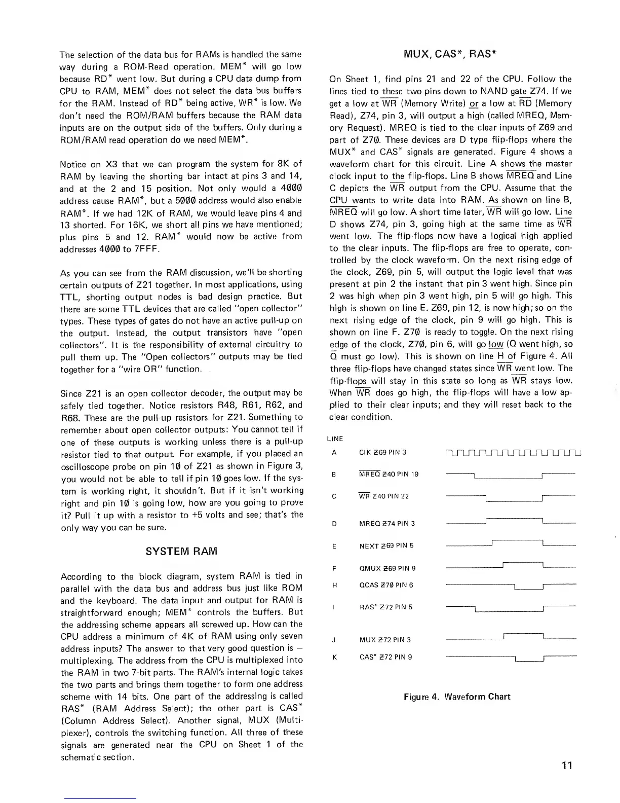
MUX, CAS*, RAS*
On Sheet
1,
find pins
21 and 22 of the
CPU. Follow the
lines tied to these two
pins down
to
NAND gate Z74. If we
get a
low
at
WR
(Memory Write)
or a
low at RD (Memory
Read), Z74, pin
3,
will output a
high (called
MREQ,
Mem-
ory
Request).
MREQ
is tied to
the clear inputs of
Z69
and
part of
Z70. These
devices
are
D type flip-flops where the
MUX* and CAS*
signals
are
generated.
Figure
4
shows
a
waveform chart
for this circuit. Line
A shows the master
clock
input
to
the flip-flops.
Line B shows
MREQ
and Line
C depicts the
WR output from the
CPU. Assume that the
CPU
wants to
write data into
RAM. As shown on line
B,
MREQ
will go low.
A short time later,
WR will
go
low. Line
D shows
Z74, pin
3,
going
high
at
the same time as
WR
went low.
The flip-flops
now have
a
logical high applied
to the clear
inputs. The flip-flops are free to
operate, con-
trolled by the clock
waveform. On the next rising edge
of
the clock,
Z69, pin
5,
will output
the logic level that was
present
at
pin 2
the instant that pin 3 went
high. Since pin
2 was
high
when
pin
3
went
high, pin 5 will go high.
This
high is shown on
line
E.
Z69, pin
12,
is now
high;
so
on the
next rising edge
of the clock, pin 9
will
go
high. This is
shown on
line
F. Z70
is ready to
toggle. On the next rising
edge of the
clock, Z70, pin
6,
will
go
low
(Q
went
high,
so
Q must go
low). This is shown
on line
H
of
Figure
4.
All
three
flip-flops
have changed states
since WR went low. The
flip-flops will stay
in this state so
long as WR stays
low.
When WR does go
high, the flip-flops
will
have a
low ap-
plied to their
clear inputs; and they
will
reset
back to the
clear
condition.
nJlJTJTJTJT_TLJT_nJlJlJTJ
LINE
A
CIK
269PIN
3
B
MREQ 240
PIN
19
C
WR 240
PIN
22
D
MREQ 274 PIN
3
E NEXT
269
PIN
5
F QMUX 269
PIN
9
H
QCAS270PIN
6
I RAS*
272 PIN 5
J MUX 272
PIN
3
K
CAS* 272
PIN
9
Figure
4. Waveform
Chart
11
 Loading...