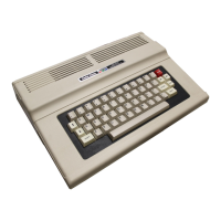
KEYBOARD
PORT ADDRESSING
The TRS-80
keyboard consists of 53 single pole, single
throw normally open keys molded in
a
plastic
base.
The
base is mounted, together with four ICs
and associated
resistors,
to
the keyboard
PCB.
As
you can see from the
schematic,
this keyboard does not output ASCII. It
is
scanned not unlike calculator
type keyboards.
Each
key
represents a switch across a matrix node. When
closed, the
switch will short out a horizontal line
to a
vertical
line.
ROM
software will detect the node short and
generate
ASCII equivalents for that particular
key.
The
keyboard is accessed by
decoder signal KYBD*.
When
this signal
goes low, it enables tristate
buffers Z3
and Z4.
The
inputs to these buffers are normally
held
high by the
pull-up resistors
at
the
top
of
the keyboard
schematic,
R1
through R8. All of the horizontal address
lines are
made
to
go
high
at
the same time
as
KYBD*
goes low. If the CPU
detects a logical
"1"
on one of the
data lines,
there is
a key
pressed on the keyboard. The
CPU
ROM
will
then scan the
address
lines
one-by-one until it finds
the
"1"
output on
the data bus again. After finding it,
the ROM
can instruct
the
CPU
how
to
generate the ASCI I
code for
that particular
key. At this time,
the
CPU
also checks
the
status of the
two
shift keys.
If
one of these keys is not
pressed,
the
ASCII
code is not modified. If a shift key is
pressed,
the ASCII is
modified accordingly.
Only one point should be brought
up about
the keyboard.
The inverters
on
the address lines
are
open collector
types.
You may not be able to see
the address
signal
on
Z1
or
Z2's
output
unless
one
of
the keys associated
with that
out-
put is pressed. With no key
pressed, there
is no voltage
applied
to
the KR (Keyboard Row)
lines.
When a key is
pressed, the associated pull-up
resistor supplies voltage.
Then you will be
able
to
see activity on
a
KR
line.
INPUT AND OUTPUT PORT
The
TRS-80 microcomputer system is
memory mapped.
But it does have input/output ports. The
basic
difference
in memory mapping and
ports is in the
method data is
handled. In
memory
mapping,
the
CPU
knows where the
data is. In a port, the
CPU
does not
know and couldn't
care where the data is located. If
the port is some
kind of
memory, the
CPU
will output data
to that
port, and it
would be up to port
circuitry
to process
and store data. In
the
input
condition, the
CPU
accesses
the input
port; and it
is up to the port to find data and feed
this data
to
the
data
bus for the
CPU.
The Z-80 CPU
can
access
up to 256 output/input
ports.
In
the
TRS-80
system, we only use
one. The
cassette
recorder is the only port used. Its
address
is
FF
in hex.
(Ports
are
accessed using only
the lower
eight address lines.)
Since the TRS-80
uses only one
output/input port,
there
must be only one
port decoder. The
port decoder is shown
on Sheet
2,
between the
sync mixing circuit
and the power
supply.
Z54
monitors
address
bits Z1
through Z7. Z52,
pin
5,
monitors
the A0 line. When hex FF
is outputted
on address
lines A0 through A8, Z54
pin
8,
and
Z52
pin
6,
will
go
low.
These
two outputs
are tied to OR
gate
Z36,
pins 2 and
1.
When A0*
and
FE*
are low,
FF*
at pin 3 of Z36
will go
low. The
port address decoding
is now complete. If
we have
a
low
at OUT* (the CPU
wants to access
an output
port
when this signal is low), Z25,
pin
8,
will output OUTSIG*
because OUT*
and_
FF*
are low. If
we
have
a low at IN*
(the CPU
wants to access
an input port), Z25,
pin
6,
will
output
a
low generating
INSIG* because
IN* and
FF*
are
low. IN*
and OUT*
should never
be active (low)
at the
same
time. Hence, INSIG*
and OUTSIG*
should never
be
active
(low)
at
the
same time.
OUTSIG*
The OUTSIG*
line is used
to control
two cassette
functions
and one video
function.
It
is used
to generate
the audio
signal for
the cassette
recorder
in
a
CSAVE
condition. It
is
used to control
the
recorder's
motor also. Its
video
function
is
to control
signal MODESEL
(Mode
Select). MODESEL
will change
64 character
format
to 32 character
format
or
vice
versa.
OUTSIG*
is
also
controlling
a latch
made
up
of
NAND
gates in Z24.
We
will discuss
this circuit
later.
Z59
is
a data latch
controlled
by OUTSIG*.
This
latch
accepts
data on lines
D0
through D3.
D0 and D1
are tied
to
pins
4
and
5
of Z59.
These
two inputs
are used
to input
data
that is recorded
on tape during
a
CSAVE
function.
D2
is
connected
to pin
12 of Z59.
This
input controls
the
status of
the recorder's
motor. D3
is
connected
to pin 18 of
Z59.
This
input
controls
the status
of MODESEL*.
The
input
to latch Z59
is
stored
and transferred
to the
output
each time
OUTSIG*
goes high (rising
edge
triggered).
For
example,
if input
D2
is high when
OUTSIG*
goes high, pin
10
of Z59
will
go high
and stay high. The
recorder's
motor will
turn
on. If
input D2
is low when
OUTSIG*
goes high,
pin
10
of Z59
will
go low
and the
recorder's
motor will
be off.
CASSETTE
MOTOR
CONTROL
At the
start of
a
CSAVE
function,
the cassette
recorder
motor must
be
turned
on. The CPU
will cause
OUTSIG*
to
go
low
and
apply
a
logical
"1
"
to
D2.
When
OUTSIG*
goes
high, the
high
on
D2
will be
transferred
and held
at pin
10
of Z59.
This
output
is connected
to
relay drive Z41,
pins
23

 Loading...