RL78/G13 CHAPTER 29 ELECTRICAL SPECIFICATIONS
R01UH0146EJ0100 Rev.1.00 990
Sep 22, 2011
Caution The pins mounted depend on the product. Refer to 2.1.1 20-pin products to 2.1.14 128-pin products,
and 2.1.15 Pins for each product (pins other than port pins).
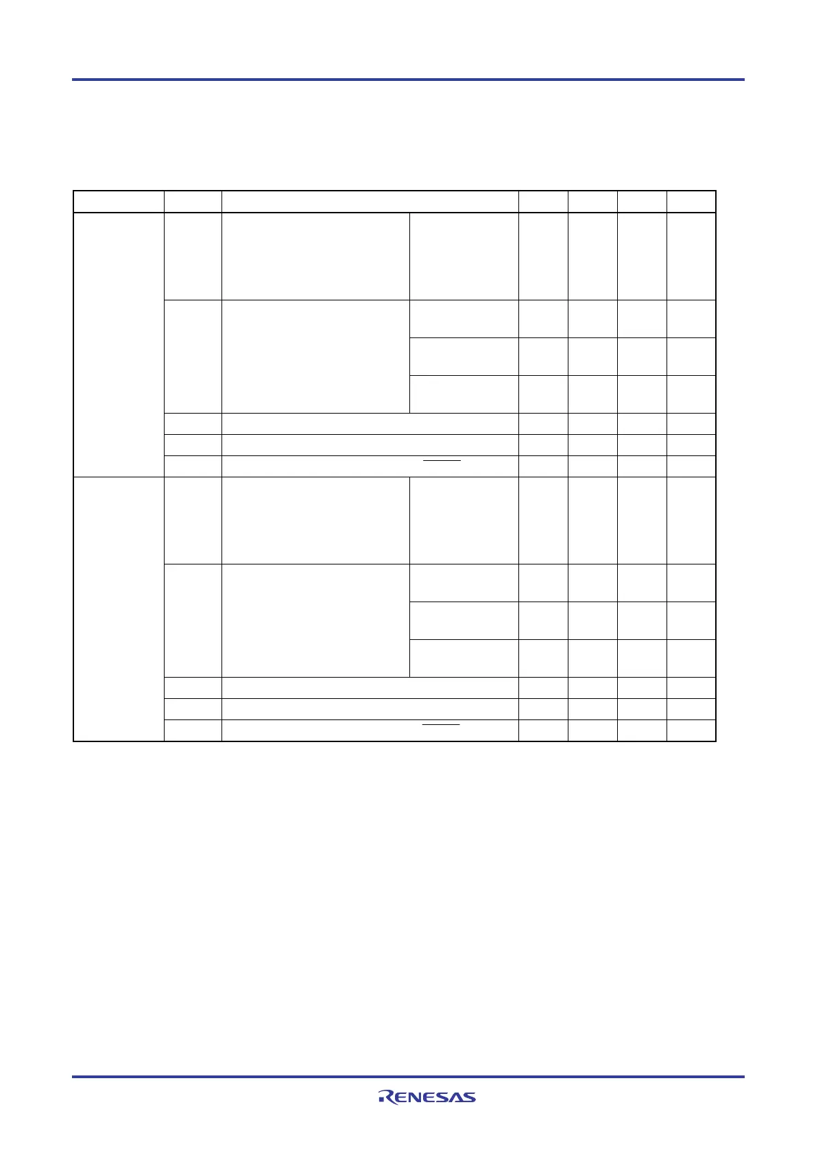
(TA = −40 to +85°C, 1.6 V ≤ EVDD0 = EVDD1 ≤ VDD ≤ 5.5 V, VSS = EVSS0 = EVSS1 = 0 V)
Items Symbol Conditions MIN. TYP. MAX. Unit
VIH1
P00 to P07, P10 to P17, P30 to P37,
P40 to P47, P50 to P57, P64 to P67,
P70 to P77, P80 to P87, P90 to P97,
P100 to P106, P110 to P117, P120,
P125 to P127, P140 to P147
Normal input buffer
0.8EV
DD0 EVDD0 V
TTL input buffer
4.0 V
≤
EV
DD0
≤
5.5 V
2.2 EVDD0 V
TTL input buffer
3.3 V
≤
EV
DD0
<
4.0 V
2.0 EVDD0 V
VIH2
P01, P03, P04, P10, P11,
P13 to P17, P43, P44, P53 to P55,
P80, P81, P142, P143
TTL input buffer
1.6 V
≤
EV
DD0
<
3.3 V
1.5 EVDD0 V
VIH3 P20 to P27, P150 to P156 0.7VDD VDD V
VIH4 P60 to P63 0.7EVDD0 6.0 V
Input voltage,
high
V
IH5 P121 to P124, P137, EXCLK, EXCLKS, RESET 0.8VDD VDD V
VIL1
P00 to P07, P10 to P17, P30 to P37,
P40 to P47, P50 to P57, P64 to P67,
P70 to P77, P80 to P87, P90 to P97,
P100 to P106, P110 to P117, P120,
P125 to P127, P140 to P147
Normal input buffer
0 0.2EV
DD0 V
TTL input buffer
4.0 V
≤
EV
DD0
≤
5.5 V
0 0.8 V
TTL input buffer
3.3 V
≤
EV
DD0
<
4.0 V
0 0.5 V
VIL2
P01, P03, P04, P10, P11,
P13 to P17, P43, P44, P53 to P55,
P80, P81, P142, P143
TTL input buffer
1.6 V
≤
EV
DD0
<
3.3 V
0 0.32 V
VIL3 P20 to P27, P150 to P156 0 0.3VDD V
VIL4 P60 to P63 0 0.3EVDD0 V
Input voltage,
low
V
IL5 P121 to P124, P137, EXCLK, EXCLKS, RESET 0 0.2VDD V
Caution The maximum value of V
IH of pins P00, P02 to P04, P10 to P15, P17, P43 to P45, P50, P52 to P55, P71,
P74, P80 to P82, P96, and P142 to P144 is EVDD0, even in the N-ch open-drain mode.
Remark Unless specified otherwise, the characteristics of alternate-function pins are the same as those of the port
pins.

 Loading...


