E1/E20/E2/E2 Lite Additional Document 2. Designing the User System
R20UT1994EJ0910 Rev.9.10 Page 33 of 59
Oct.06.23
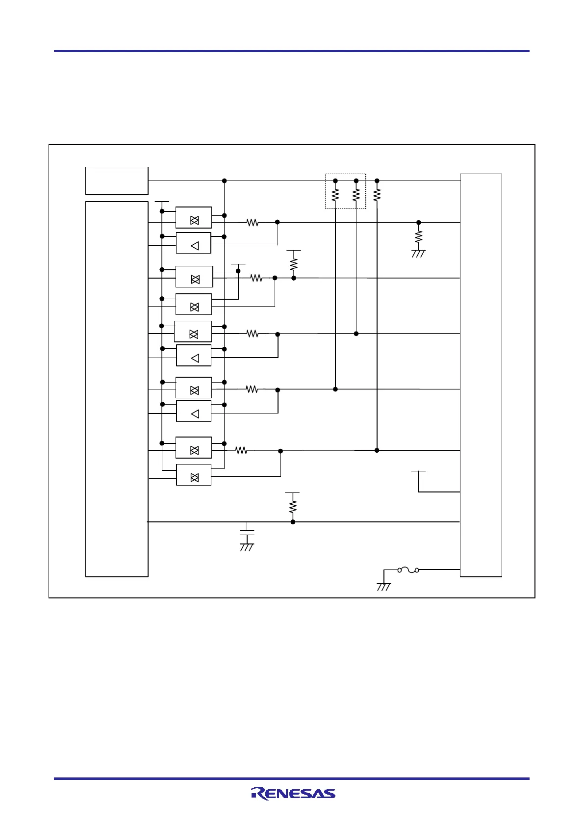
2.6.3 Internal Circuits of the E2 (when the RL78 Family is Connected)
Figure 2-18 and Figure 2-19 respectively show the internal circuits of product revisions C and D of the E2
with the RL78 family connected.
The alphabet at the end of the serial No. written on the E2 main unit indicates the product revision.
3 MΩ
RSTPU
VDD
4
8
3.3 V
EMVDD
TOOL0
5
EMVDD
6
RESET_IN
10
RESET_OUT
3.3 V
100 kΩ
GND
14
13
RESET_OUT
2,12
GND
EMVDD
EMVDD
9
1 MΩ
74 LV C1T45
74 LV C1T45
74 LV C1T45
74 LV C1T45
74 LV C1T45
0.1 µF
100 k
Ω
74 LV C1T45
Emulator
cont rol
circuit
Po w er-supply circuit
(only for use in the mode to
supply power to the user
sy stem)
User-side
connector
Sel f-recovering
fuse
47 Ω
47 Ω
47 Ω
47 Ω
47 Ω
1 MΩ × 2
74LVC 1T45
74LVC 8T245
74LVC 8T245
74LVC 8T245
Figure 2-18 Internal Circuits of the E2 (Rev. C)
Set the switch on the 20-pin (1.27-mm pin spacing) to 14-pin (2.54-mm pin spacing) connector conversion
adapter to position “3”.

 Loading...


