RL78/G13 CHAPTER 29 ELECTRICAL SPECIFICATIONS
R01UH0146EJ0100 Rev.1.00 1010
Sep 22, 2011
Caution The pins mounted depend on the product. Refer to 2.1.1 20-pin products to 2.1.14 128-pin products,
and 2.1.15 Pins for each product (pins other than port pins).
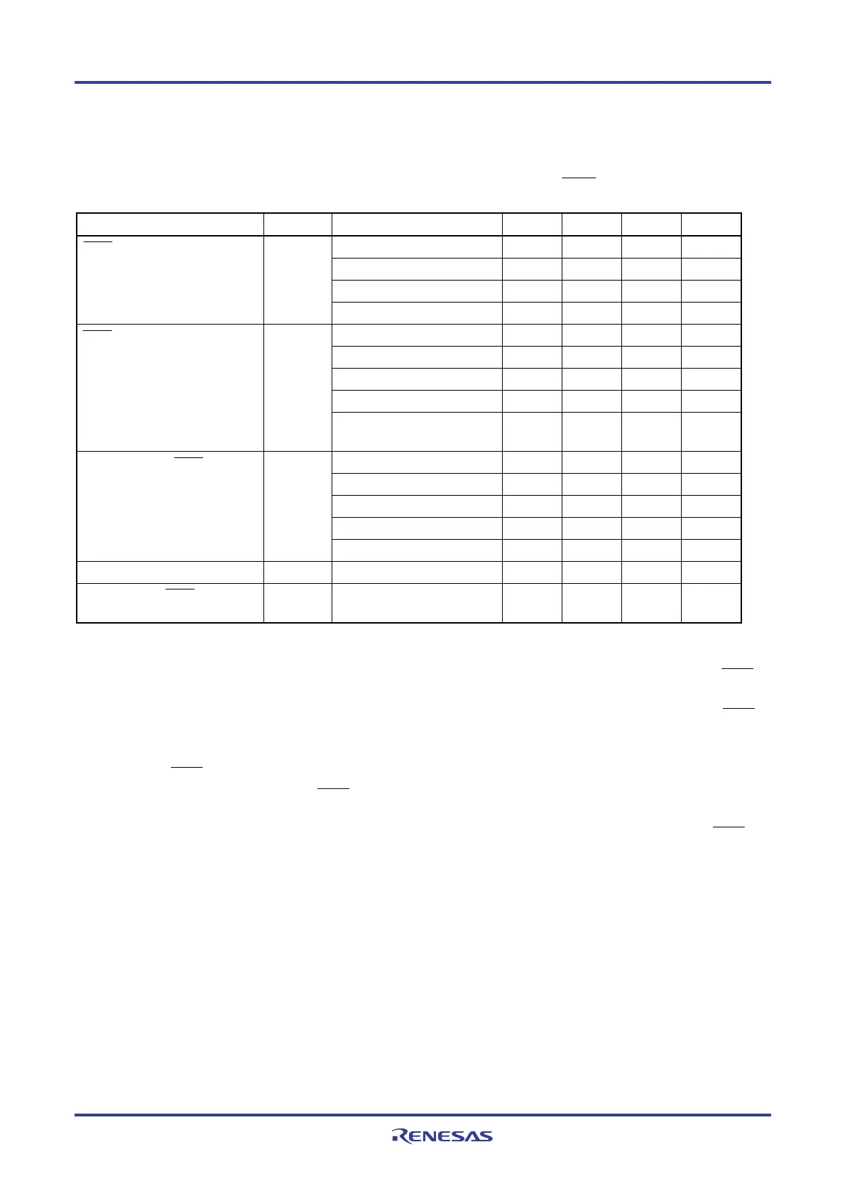
(3) During communication at same potential (CSI mode) (master mode (f
MCK/4), SCKp... internal clock output)
(TA = −40 to +85°C, 1.6 V ≤ EVDD0 = EVDD1 ≤ VDD ≤ 5.5 V, VSS = EVSS0 = EVSS1 = 0 V)
Notes 1. The value must also be 4/fCLK or more.
2. When DAPmn = 0 and CKPmn = 0, or DAPmn = 1 and CKPmn = 1. The SIp setup time becomes “to SCKp↓”
when DAPmn = 0 and CKPmn = 1, or DAPmn = 1 and CKPmn = 0.
3. When DAPmn = 0 and CKPmn = 0, or DAPmn = 1 and CKPmn = 1. The SIp hold time becomes “from SCKp↓”
when DAPmn = 0 and CKPmn = 1, or DAPmn = 1 and CKPmn = 0.
4. When DAPmn = 0 and CKPmn = 0, or DAPmn = 1 and CKPmn = 1. The delay time to SOp output becomes
“from SCKp↑” when DAPmn = 0 and CKPmn = 1, or DAPmn = 1 and CKPmn = 0.
5. C is the load capacitance of the SCKp and SOp output lines.
Caution Select the normal input buffer for the SIp pin and the normal output mode for the SOp pin and SCKp pin
by using port input mode register g (PIMg) and port output mode register g (POMg).
Remarks 1. This specification is valid only when CSI00’s peripheral I/O redirect function is not used.
2. p: CSI number (p = 00, 01, 10, 11, 20, 21, 30, 31), m: Unit number (m = 0, 1), n: Channel number (n = 0 to 3),
g: PIM and POM numbers (g = 0, 1, 4, 5, 8, 14)
3. f
MCK: Serial array unit operation clock frequency
(Operation clock to be set by the CKSmn bit of serial mode register mn (SMRmn). m: Unit number,
n: Channel number (mn = 00 to 03, 10 to 13))
Parameter Symbol Conditions MIN. TYP. MAX. Unit
2.7 V ≤ EVDD0 ≤ 5.5 V 125
Note 1
ns
2.4 V ≤ EVDD0 ≤ 5.5 V 250
Note 1
ns
1.8 V ≤ EVDD0 ≤ 5.5 V 500
Note 1
ns
SCKp cycle time tKCY1
1.6 V ≤ EV
DD0 ≤ 5.5 V 1000
Note 1
ns
4.0 V ≤ EVDD0 ≤ 5.5 V tKCY1/2 − 12 ns
2.7 V ≤ EVDD0 ≤ 5.5 V tKCY1/2 − 18 ns
2.4 V ≤ EVDD0 ≤ 5.5 V tKCY1/2 − 38 ns
1.8 V ≤ EVDD0 ≤ 5.5 V tKCY1/2 − 50 ns
SCKp high-/low-level width
t
KH1,
t
KL1
1.6 V ≤ EV
DD0 ≤ 5.5 V
t
KCY1/2 −
100
ns
4.0 V ≤ EVDD0 ≤ 5.5 V 44 ns
2.7 V ≤ EVDD0 ≤ 5.5 V 44 ns
2.4 V ≤ EVDD0 ≤ 5.5 V 75 ns
1.8 V ≤ EVDD0 ≤ 5.5 V 110 ns
SIp setup time (to SCKp↑)
Note 2
tSIK1
1.6 V ≤ EV
DD0 ≤ 5.5 V 220 ns
SIp hold time (from SCKp↑)
Note 3
tKSI1 19 ns
Delay time from SCKp↓ to
SOp output
Note 4
t
KSO1 C = 30 pF
Note 5
25 ns
<R>

 Loading...


