RL78/G13 CHAPTER 29 ELECTRICAL SPECIFICATIONS
R01UH0146EJ0100 Rev.1.00 1014
Sep 22, 2011
Caution The pins mounted depend on the product. Refer to 2.1.1 20-pin products to 2.1.14 128-pin products,
and 2.1.15 Pins for each product (pins other than port pins).
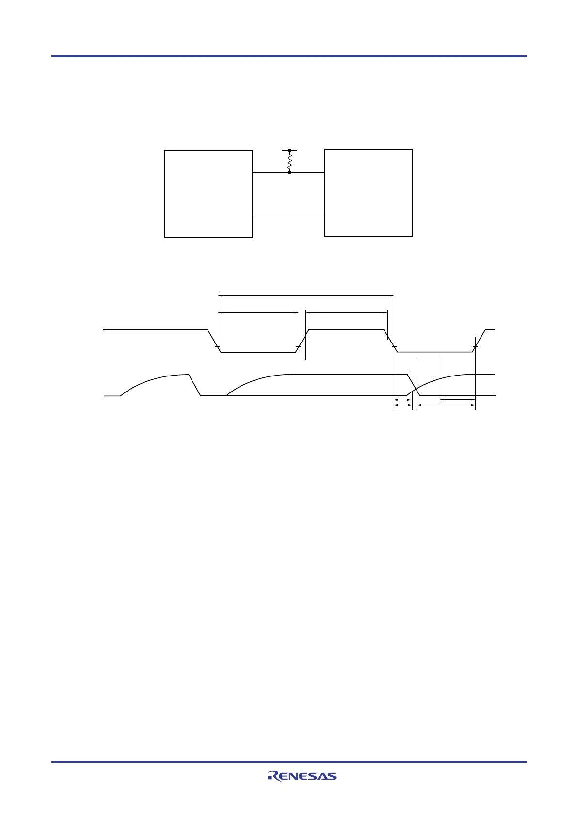
Simplified I
2
C mode mode connection diagram (during communication at same potential)
User's device
SDAr
SCLr
SDA
SCL
V
DD
R
b
RL78/G13
Simplified I
2
C mode serial transfer timing (during communication at same potential)
SDAr
t
LOW
tHIGH
tHD:DAT
SCLr
t
SU:DAT
1/fSCL
Caution Select the TTL input buffer and the N-ch open drain output (VDD tolerance) mode for the SDAr pin and
the normal output mode for the SCLr pin by using port input mode register g (PIMg) and port output
mode register h (POMh).
Remarks 1. R
b[Ω]:Communication line (SDAr) pull-up resistance, Cb[F]: Communication line (SDAr, SCLr) load
capacitance
2. r: IIC number (r = 00, 01, 10, 11, 20, 21, 30, 31), g: PIM number (g = 0, 1, 4, 5, 8, 14),
h: POM number (g = 0, 1, 4, 5, 7 to 9, 14)
3. f
MCK: Serial array unit operation clock frequency
(Operation clock to be set by the CKSmn bit of serial mode register mn (SMRmn). m: Unit number (m = 0, 1),
n: Channel number (n = 0 to 3), mn = 00 to 03, 10 to 13)

 Loading...


