RL78/G13 CHAPTER 29 ELECTRICAL SPECIFICATIONS
R01UH0146EJ0100 Rev.1.00 1025
Sep 22, 2011
Caution The pins mounted depend on the product. Refer to 2.1.1 20-pin products to 2.1.14 128-pin products,
and 2.1.15 Pins for each product (pins other than port pins).
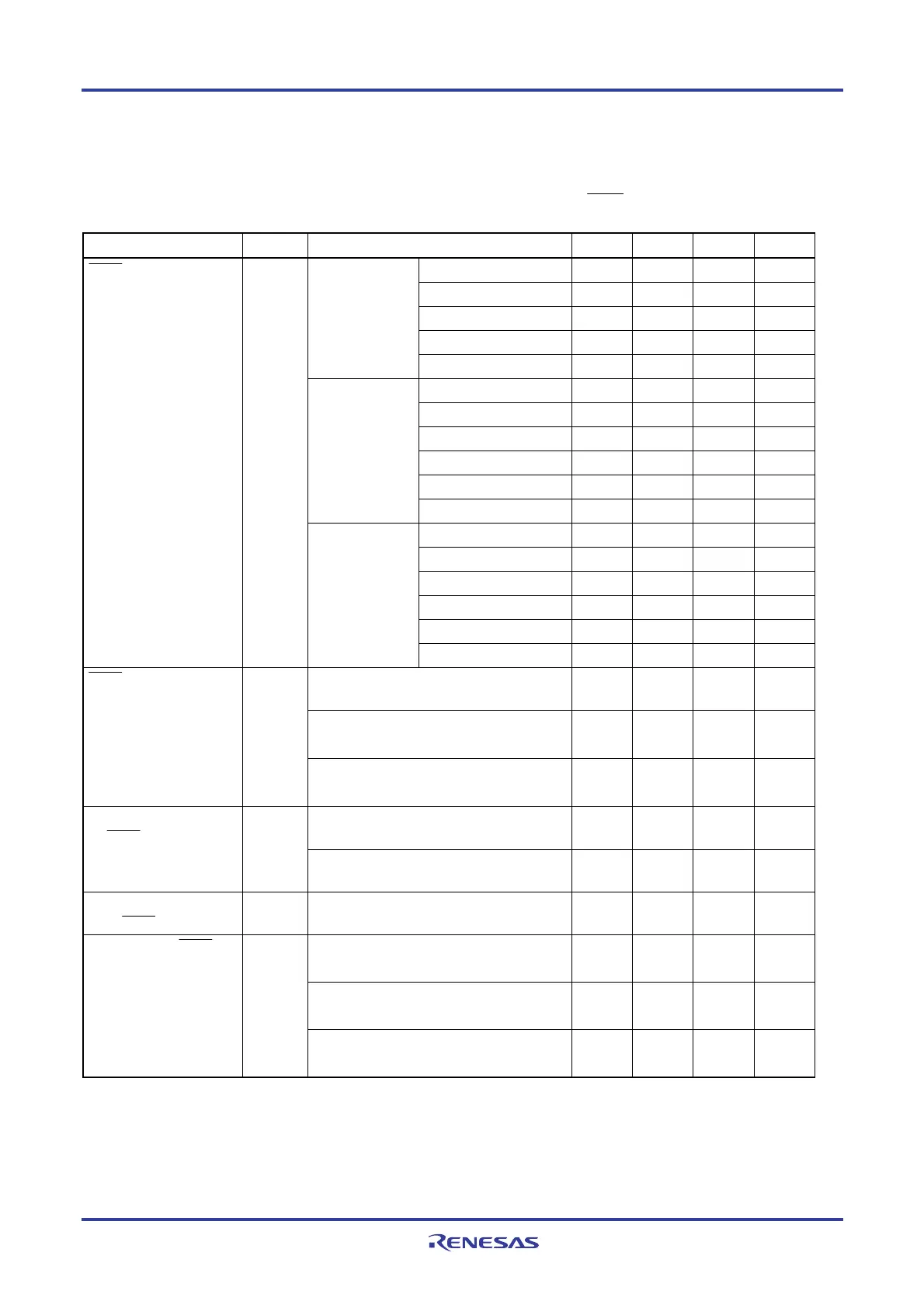
(9) Communication at different potential (2.5 V, 3 V) (CSI mode) (slave mode, SCKp... external clock input)
(T
A = −40 to +85°C, 1.8 V ≤ EVDD0 = EVDD1 ≤ VDD ≤ 5.5 V, VSS = EVSS0 = EVSS1 = 0 V)
Parameter Symbol Conditions MIN. TYP. MAX. Unit
24 MHz < fMCK 14/fMCK ns
20 MHz < fMCK ≤ 24 MHz 12/fMCK ns
8 MHz < fMCK ≤ 20 MHz 10/fMCK ns
4 MHz < fMCK ≤ 8 MHz 8/fMCK ns
4.0 V
≤
EV
DD0
≤
5.5 V,
2.7 V
≤
V
b
≤
4.0 V
f
MCK ≤ 4 MHz 6/fMCK ns
24 MHz < fMCK 20/fMCK ns
20 MHz < fMCK ≤ 24 MHz 16/fMCK ns
16 MHz < fMCK ≤ 20 MHz 14/fMCK ns
8 MHz < fMCK ≤ 16 MHz 12/fMCK ns
4 MHz < fMCK ≤ 8 MHz
8/fMCK ns
2.7 V
≤
EV
DD0
< 4.0 V,
2.3 V
≤
V
b
≤
2.7 V
f
MCK ≤ 4 MHz
6/fMCK ns
24 MHz < fMCK 48/fMCK ns
20 MHz < fMCK ≤ 24 MHz 36/fMCK ns
16 MHz < fMCK ≤ 20 MHz 32/fMCK ns
8 MHz < fMCK ≤ 16 MHz 26/fMCK ns
4 MHz < fMCK ≤ 8 MHz
16/fMCK ns
SCKp cycle time
Note 1
tKCY2
1.8 V
≤
EV
DD0
< 3.3 V,
1.6 V
≤
V
b
≤
2.0 V
Note 2
fMCK ≤ 4 MHz
10/fMCK ns
4.0 V ≤ EVDD0 ≤ 5.5 V, 2.7 V ≤ Vb ≤ 4.0 V
t
KCY2/2 −
12
ns
2.7 V ≤ EVDD0 < 4.0 V, 2.3 V ≤ Vb ≤ 2.7 V
t
KCY2/2 −
18
ns
SCKp high-/low-level
width
tKH2,
t
KL2
1.8 V ≤ EV
DD0 < 3.3 V, 1.6 V ≤ Vb ≤ 2.0 V
Note 2
t
KCY2/2 −
50
ns
2.7 V ≤ EVDD0 ≤ 5.5 V
1/f
MCK +
20
ns
SIp setup time
(to SCKp↑)
Note 3
t
SIK2
1.8 V ≤ EV
DD0 < 3.3 V
1/f
MCK +
30
ns
SIp hold time
(from SCKp↑)
Note 4
t
KSI2 1/fMCK + 31 ns
4.0 V ≤ EVDD0 ≤ 5.5 V, 2.7 V ≤ Vb ≤ 4.0 V,
C
b = 30 pF, Rb = 1.4 kΩ
1/f
MCK +
250
2/f
MCK +
120
ns
2.7 V ≤ EVDD0 < 4.0 V, 2.3 V ≤ Vb ≤ 2.7 V,
C
b = 30 pF, Rb = 2.7 kΩ
2/f
MCK +
214
ns
Delay time from SCKp↓ to
SOp output
Note 5
t
KSO2
1.8 V ≤ EV
DD0 < 3.3 V, 1.6 V ≤ Vb ≤ 2.0 V
Note 2
,
C
b = 30 pF, Rb = 5.5 kΩ
2/f
MCK +
573
ns
(Notes, Caution and Remarks are listed on the next page.)
<R>
<R>
<R>

 Loading...


