RL78/G13 CHAPTER 29 ELECTRICAL SPECIFICATIONS
R01UH0146EJ0100 Rev.1.00 1027
Sep 22, 2011
Caution The pins mounted depend on the product. Refer to 2.1.1 20-pin products to 2.1.14 128-pin products,
and 2.1.15 Pins for each product (pins other than port pins).
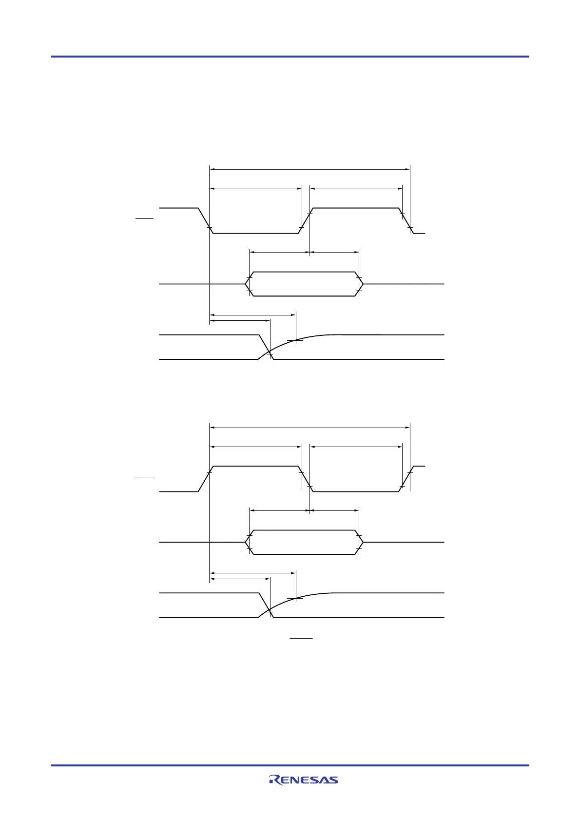
CSI mode serial transfer timing (slave mode) (during communication at different potential)
(When DAPmn = 0 and CKPmn = 0, or DAPmn = 1 and CKPmn = 1.)
SIp Input data
Output data
SOp
t
KCY2
t
KL2
t
KH2
t
SIK2
t
KSI2
t
KSO2
SCKp
CSI mode serial transfer timing (slave mode) (during communication at different potential)
(When DAPmn = 0 and CKPmn = 1, or DAPmn = 1 and CKPmn = 0.)
SIp Input data
Output data
SOp
t
KCY2
t
KL2
t
KH2
t
SIK2
t
KSI2
t
KSO2
SCKp
Caution Select the TTL input buffer for the SIp pin and SCKp pin and the N-ch open drain output (VDD tolerance)
mode for the SOp pin by using port input mode register g (PIMg) and port output mode register g
(POMg).
Remarks 1. p: CSI number (p = 00, 01, 10, 20, 30, 31), m: Unit number, n: Channel number (mn = 00, 01, 02, 10, 12. 13),
g: PIM and POM number (g = 0, 1, 4, 5, 8, 14)
2. CSI01 of 48-, 52-, 64-pin products, and CSI11 and CSI21 cannot communicate at different potential. Use
other CSI for communication at different potential.

 Loading...


