RL78/G13 CHAPTER 29 ELECTRICAL SPECIFICATIONS
R01UH0146EJ0100 Rev.1.00 1029
Sep 22, 2011
Caution The pins mounted depend on the product. Refer to 2.1.1 20-pin products to 2.1.14 128-pin products,
and 2.1.15 Pins for each product (pins other than port pins).
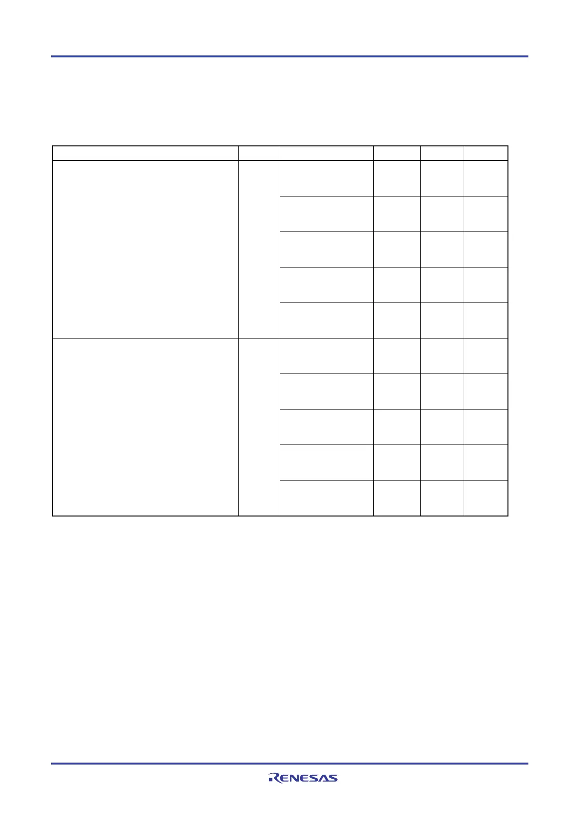
(10) Communication at different potential (2.5 V, 3 V) (simplified I
2
C mode) (2/2)
(T
A = −40 to +85°C, 1.8 V ≤ EVDD0 = EVDD1 ≤ VDD ≤ 5.5 V, VSS = EVSS0 = EVSS1 = 0 V)
Parameter Symbol Conditions MIN. MAX. Unit
4.0 V ≤ EVDD0 ≤ 5.5 V,
2.7 V ≤ V
b ≤ 4.0 V,
C
b = 50 pF, Rb = 2.7 kΩ
1/f
MCK + 135
Note 2
ns
2.7 V ≤ EVDD0 < 4.0 V,
2.3 V ≤ V
b < 2.7 V,
C
b = 50 pF, Rb = 2.7 kΩ
1/f
MCK + 135
Note 2
ns
4.0 V ≤ EVDD0 ≤ 5.5 V,
2.7 V ≤ V
b ≤ 4.0 V,
C
b = 100 pF, Rb = 2.8 kΩ
1/f
MCK + 190
Note 2
ns
2.7 V ≤ EVDD0 < 4.0 V,
2.3 V ≤ V
b < 2.7 V,
C
b = 100 pF, Rb = 2.7 kΩ
1/f
MCK + 190
Note 2
ns
Data setup time (reception) tSU:DAT
1.8 V ≤ EV
DD0 < 3.3 V,
1.6 V ≤ V
b ≤ 2.0 V
Notes 1
,
C
b = 100 pF, Rb = 5.5 kΩ
1/f
MCK + 190
Note 2
ns
4.0 V ≤ EVDD0 ≤ 5.5 V,
2.7 V ≤ V
b ≤ 4.0 V,
C
b = 50 pF, Rb = 2.7 kΩ
0 305 ns
2.7 V ≤ EVDD0 < 4.0 V,
2.3 V ≤ V
b < 2.7 V,
C
b = 50 pF, Rb = 2.7 kΩ
0 305 ns
4.0 V ≤ EVDD0 ≤ 5.5 V,
2.7 V ≤ V
b ≤ 4.0 V,
C
b = 100 pF, Rb = 2.8 kΩ
0 355 ns
2.7 V ≤ EVDD0 < 4.0 V,
2.3 V ≤ V
b < 2.7 V,
C
b = 100 pF, Rb = 2.7 kΩ
0 355 ns
Data hold time (transmission) tHD:DAT
1.8 V ≤ EV
DD0 < 3.3 V,
1.6 V ≤ V
b ≤ 2.0 V
Note 1
,
C
b = 100 pF, Rb = 5.5 kΩ
0 405 ns
Notes 1. Use it with EVDD0 ≥ Vb.
2. Set the fMCK value to keep the hold time of SCLr = "L" and SCLr = "H".
Caution Select the TTL input buffer and the N-ch open drain output (V
DD tolerance) mode for the SDAr pin and
the N-ch open drain output (VDD tolerance) mode for the SCLr pin by using port input mode register g
(PIMg) and port output mode register g (POMg).
(Remarks is listed on the next page.)
<R>
<R>
<R>
<R>

 Loading...


