RL78/G13 CHAPTER 3 CPU ARCHITECTURE
R01UH0146EJ0100 Rev.1.00 99
Sep 22, 2011
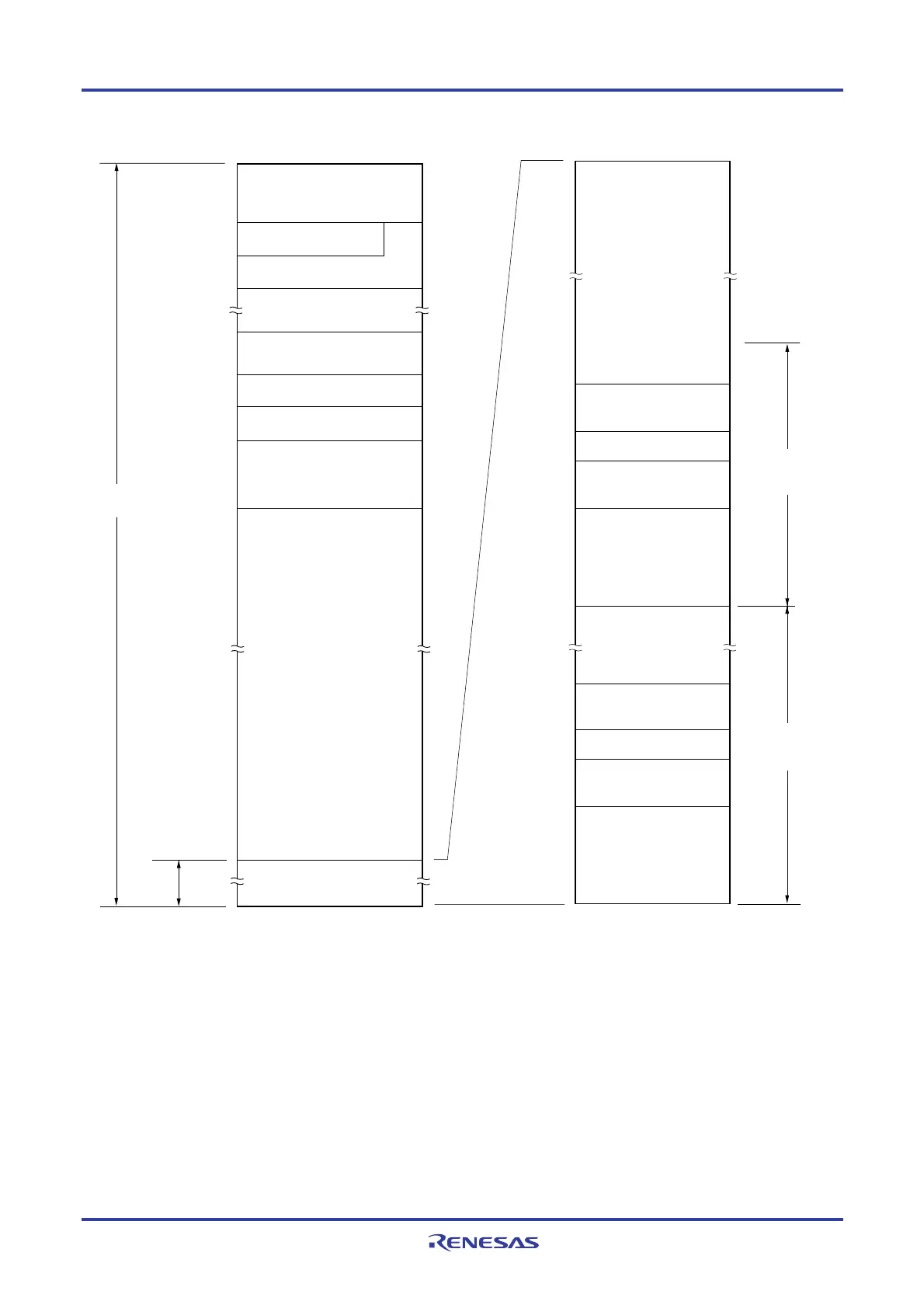
Figure 3-1. Memory Map (R5F100xA, R5F101xA(x = 6 to 8, A to C, E to G))
Special function register (SFR)
256 bytes
General-purpose register
32 bytes
RAM
Note 1
2 KB
Reserved
Special function register (2nd SFR)
2 KB
Reserved
Code flash memory
16 KB
Data memory
space
Program
memory
space
00000H
EFFFFH
F0000H
F0FFFH
F1000H
Data flash memory
Note 4
4 KB
F1FFFH
F2000H
FF6FFH
FF700H
FFEDFH
FFEE0H
FFEFFH
FFF00H
FFFFFH
03FFFH
04000H
F07FFH
F0800H
00000H
0007FH
00080H
000BFH
000C0H
000C3H
000C4H
00FFFH
01000H
0107FH
01080H
010BFH
010C0H
010C3H
010C4H
03FFFH
Vector table area
128 bytes
CALLT table area
64 bytes
Program area
Option byte area
Note 2
4 bytes
Vector table area
128 bytes
CALLT table area
64 bytes
Option byte area
Note 2
4 bytes
Program area
On-chip debug security
ID setting area
Note 2
10 bytes
01FFFH
Boot cluster 0
Note 3
Boot cluster 1
010CDH
010CEH
On-chip debug security
ID setting area
Note 2
10 bytes
000CDH
000CEH
Mirror
8 KB
Reserved
F3FFFH
F4000H
Notes 1. Instructions can be executed from the RAM area excluding the general-purpose register area.
2. When boot swap is not used: Set the option bytes to 000C0H to 000C3H, and the on-chip debug security
IDs to 000C4H to 000CDH.
When boot swap is used: Set the option bytes to 000C0H to 000C3H and 010C0H to 010C3H, and the
on-chip debug security IDs to 000C4H to 000CDH and 010C4H to 010CDH.
3. Writing boot cluster 0 can be prohibited depending on the setting of security (see 25.6 Security Setting).
4. R5F100xA only.
Caution When executing instructions from the RAM area while RAM parity error resets are enabled (RPERDIS
= 1), be sure to initialize the used RAM area + 10 bytes.
<R>

 Loading...


