RL78/G13 CHAPTER 11 A/D CONVERTER
R01UH0146EJ0100 Rev.1.00 497
Sep 22, 2011
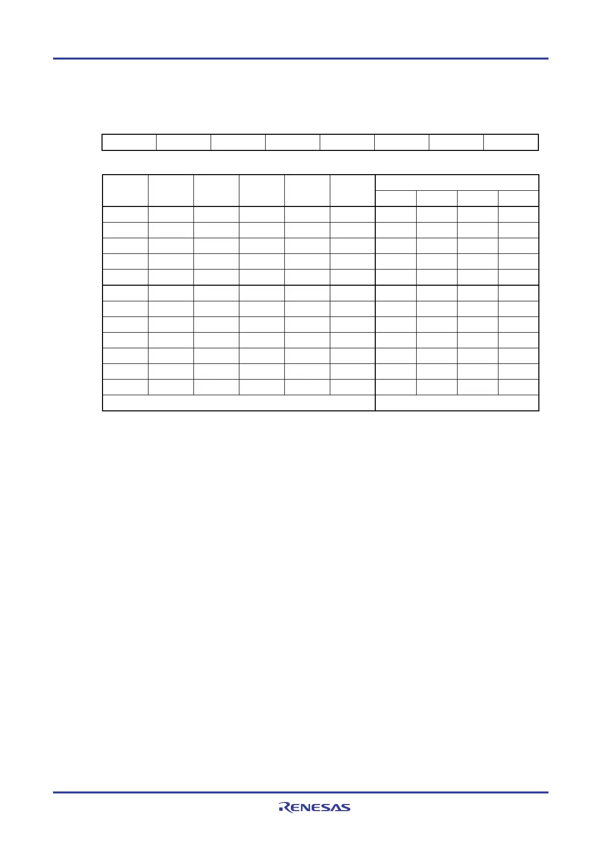
Figure 11-11. Format of Analog Input Channel Specification Register (ADS) (2/2)
Address: FFF31H After reset: 00H R/W
Symbol 7 6 5 4 3 2 1 0
ADS ADISS 0 0 ADS4 ADS3 ADS2 ADS1 ADS0
{ Scan mode (ADMD = 1)
Analog input channel ADISS ADS4 ADS3 ADS2 ADS1 ADS0
Scan 0 Scan 1 Scan 2 Scan 3
0 0 0 0 0 0 ANI0 ANI1 ANI2 ANI3
0 0 0 0 0 1 ANI1 ANI2 ANI3 ANI4
0 0 0 0 1 0 ANI2 ANI3 ANI4 ANI5
0 0 0 0 1 1 ANI3 ANI4 ANI5 ANI6
0 0 0 1 0 0 ANI4 ANI5 ANI6 ANI7
0 0 0 0 0 0 ANI5 ANI6 ANI7 ANI8
0 0 0 0 0 1 ANI6 ANI7 ANI8 ANI9
0 0 0 0 1 0 ANI7 ANI8 ANI9 ANI10
0 0 0 0 1 1 ANI8 ANI9 ANI10 ANI11
0 0 0 0 1 0 ANI9 ANI10 ANI11 ANI12
0 0 0 0 1 1 ANI10 ANI11 ANI12 ANI13
0 0 0 1 0 0 ANI11 ANI12 ANI13 ANI14
Other than the above Setting prohibited
Cautions 1. Be sure to clear bits 5 and 6 to 0.
2 Set a channel to be used for A/D conversion in the input mode by using port mode registers 0, 2,
3, 10 to 12, 14, or 15 (PM0, PM2, PM3, PM10 t o PM12, PM14, PM15).
3. Do not set the pin that is set by the A/D port configuration register (ADPC) as digital I/O by the
ADS register.
4. Do not set the pin that is set by port mode control register 0, 3, 10 to 12, or 14 (PMC0, PMC3,
PMC10 to PMC12, PMC14) as digital I/O by the ADS register.
5. Only rewrite the value of the ADISS bit while conversion operation is stopped (which is indicated
by the ADCE bit of A/D voltage cooperator mode register 0 (ADM0) being 0).
6. If using AV
REFP as the + side reference voltage source of the A/D converter, do not select ANI0 as
an A/D conversion channel.
7. If using AV
REFM as the − side reference voltage source of the A/D converter, do not select ANI1 as
an A/D conversion channel.
8. If ADISS is set to 1, the internal reference voltage (1.45 V) cannot be used for the + side reference
voltage source.
Remark ×: don’t care
<R>
<R>

 Loading...


