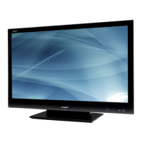
LC-32/40/46LE700E/RU/S,LU700E/S,LX700E/RU,LC-52LE700E/RU/S
7 – 26
18 R2X2P I
17 R2X2N I
12 R2XCP I TMDS input port 2 clock pair
11 R2XCN I
22 R3X0P I TMDS input port 3 data pairs.
21 R3X0N I
24 R3X1P I
23 R3X1N I
26 R3X2P I
25 R3X2N I
20 R3XCP I TMDS input port 3 clock pair
19 R3XCN I
HDMI Tx Port Pins
60 TX0P O HDMI Tx Output port data.
61 TX0N O TMDS Low Voltage Differential Signal output data pairs.
58 TX1P O
59 TX1N O
56 TX2P O
57 TX2N O
62 TXCP O HDMI Output port Clock.
63 TXCN O TMDS Low Voltage Differential Signal output data pairs.
System Switching Pins
29 DSDA0 I/O DDC I2C Data for respective port.
These signals are true open drain, and do not pull-down to ground when power is not applied to the device.
These pins require an external pull-up resistor.
33 DSDA1 I/O
39 DSDA2 I/O
43 DSDA3 I/O
30 DSCL0 I
DDC I2C Clock for respective port.
These signals are true open drain, and do not pull-down to ground when power is not applied to the device.
These pins require an external pull-up resistor.
34 DSCL1 I
40 DSCL2 I
44 DSCL3 I
32 R0PWR5V -
5-V Port detection input for respective port.
Connect to 5-V signal from HDMI input connector.
These signals require a 10Ω series resistor and at least a 1µ F capacitor to ground A 3.3kΩ pull-down resis-
tor is also required for these signals.
36 R1PWR5V -
42 R2PWR5V -
46 R3PWR5V -
31 CBUS_HPD0 O
Hot Plug Detect Output for respective port.
Connect to HOTPLUG of HDMI input connector.In MHL mode, this serves at the respective port control bus.
35 CBUS_HPD1 O
41 CBUS_HPD2 O
45 CBUS_HPD3 O
49 R4PWR5V - 5V power from 5th Rx port.
Control Pins
54 CSCL I
Local Configuration/Status I2C Clock.
Chip configuration/status is accessed via this I2C port. This pin is a true open drain, so it does not pull to
ground if power is not applied.
53 CSDA I/O
Local Configuration/Status I2C Data.
Chip configuration/status is accessed via this I2C port. This pin is a true open drain, so it does not pull to
ground if power is not applied.
48 DSCL4 I
DDC I2C Clock for VGA port.
These signals are true open drain, and do not pull-down to ground when power is not applied to the device.
This pin requires an external pull-up resister.
47 DSDA4 I/O
DDC I2C Data for VGA port.
These signals are true open drain, and do not pull-down to ground when power is not applied to the device.
This pin requires an external pull-up resister.
Configurations Pins
55 TPWR_CI2CA I/O
I2C Slave Address input/Transmit Power Sense Output.
At the end of power -on-reset (POR), this pin is used as an input to latch the I2C sub-address. The level on
this pin is latched when the POR transitions from the asscred state to the de-asserted state. After complec-
tion of POR, this pin is used as the TPWR output, indicating that the selected HDMI input port is receiving an
active TMDS clock. This pin has an internal pull-up to the MICOMVCC33 power supply. If this signal is
pulled-down, a 4.7LΩ resister should be used.
Note: There is a probability the POR logic may power up and not latch the level on this pin. A software
workaround is required to determine the proper I2C slave address.
52 INT O
Interrupt Output.
This is an open_drain output and requires an external pull_up resister.
10 RSVD -
When SBVCC(pin38)=5V, RSVD pin #10 must be tied to GND with less than 10K resistor. When
SBVCC(pin38)=3.3V, RSVD pin #10 must be tied to GND with 1M ohm resistor.
28 RSVD -
Pin No. Pin Name I/O Pin Function