4 Signal description 02.05
© Siemens AG 1998 All Rights Reserved
4-4 FM-STEPDRIVE/SIMOSTEP (FB)
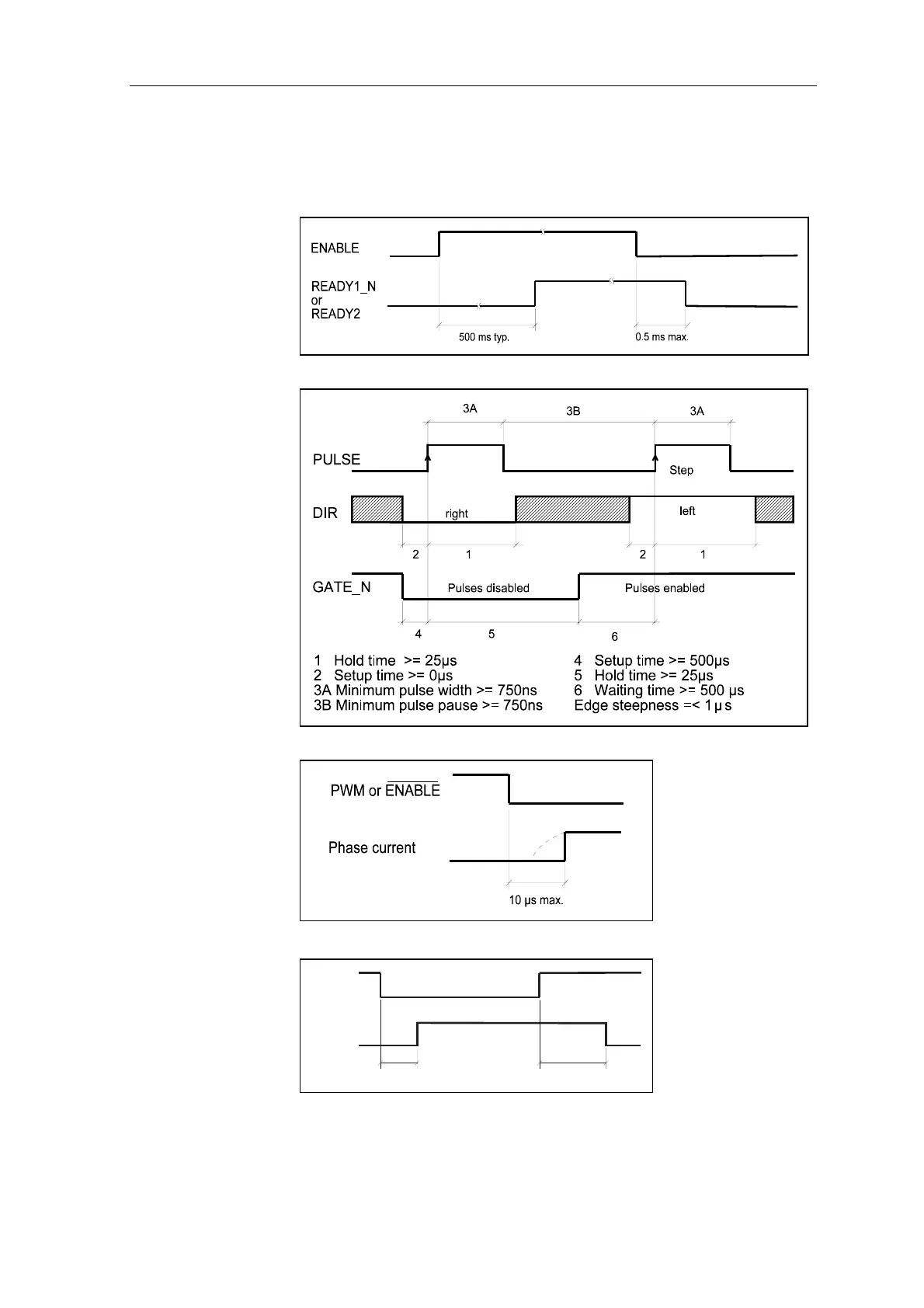
4.3 Signal timing diagrams
The timing diagrams below illustrate the timing of the input/output signals
of the pulse and signal interfaces.
Figure 4-1 ENABLE/READY timing diagram
Figure 4-2 PULSE/DIR/GATE_N timing diagram
Figure 4-3 PWM or ENABLE and motor phase current timing diagram
100ms 180ms
GATE_N
MSTILL
Figure 4-4 GATE_N/MSTILL timing diagram