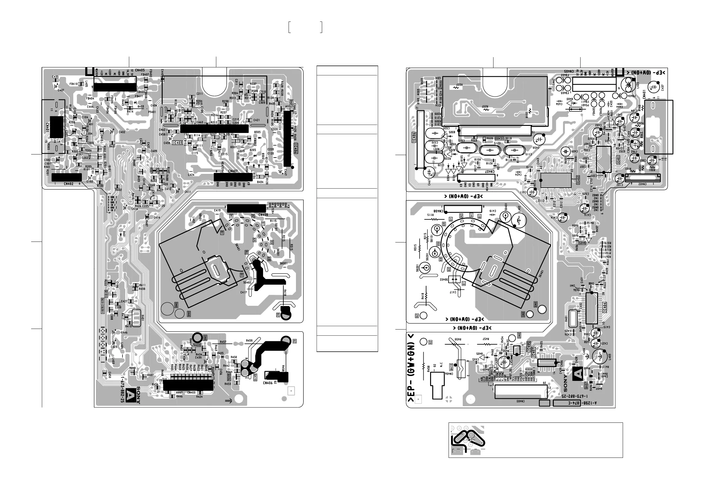
IC
IC401 B-3
IC402 B-2
IC403 A-2 A-2
IC404 C-3
IC405 D-2
IC406 A-3 A-1
IC407 D-2
TRANSISTOR
*
Q101 C-1 1
Q201 C-1 1
Q301 C-1 1
Q401 A-3 1
Q402 D-3 qg
Q406 D-3 1
Q407 D-2 2
Q410 D-3 D-1 –
DIODE
*
D101 B-1 6
D102 A-3 7
D103 A-1 qa
D105 B-3 B-1 –
D106 A-2 3
D107 A-2 3
D201 B-1 6
D202 A-3 7
D203 A-1 qa
D205 B-3 A-1 –
D206 A-1 3
D207 A-2 3
D301 B-1 6
D302 A-1 6
D303 A-1 qa
D305 A-3 A-1 –
D306 A-1 3
D307 A-3 3
D402 D-3 9
D403 A-2 A-2 –
D405 D-3 D-1 –
D406 D-2 6
D407 D-2 6
CRYSTAL
X401 C-2 C-2
Component
()
Side
5-15 5-16
Schematic diagram
<
(a)(a)
(a)(a)
(a) board
— A BOARD (Component Side) —
— A BOARD (Conductor Side) —
(a)
VIDEO AMP
RGB OUT
Conductor
()
Side
• A BOARD
SEMICONDUCTOR
LOCATION
Component
()
Side
Conductor
()
Side
*
: Refer to Terminal name of
semiconductors in silk screen
printed circuit (see page 5-10)
Component
()
Side
Conductor
()
Side
NOTE:
The circuit indicated as left contains high voltage of over
600 Vp-p. Care must be paid to prevent an electric shock in
inspection or repairing.
A
B
C
D
1 2 3
A
B
C
D
1 2 3
Component
()
Side
Conductor
()
Side
 Loading...