Smart Machine Smart Decision
SIM7020_Hardware_Design_V1.02 31 2018-07-25
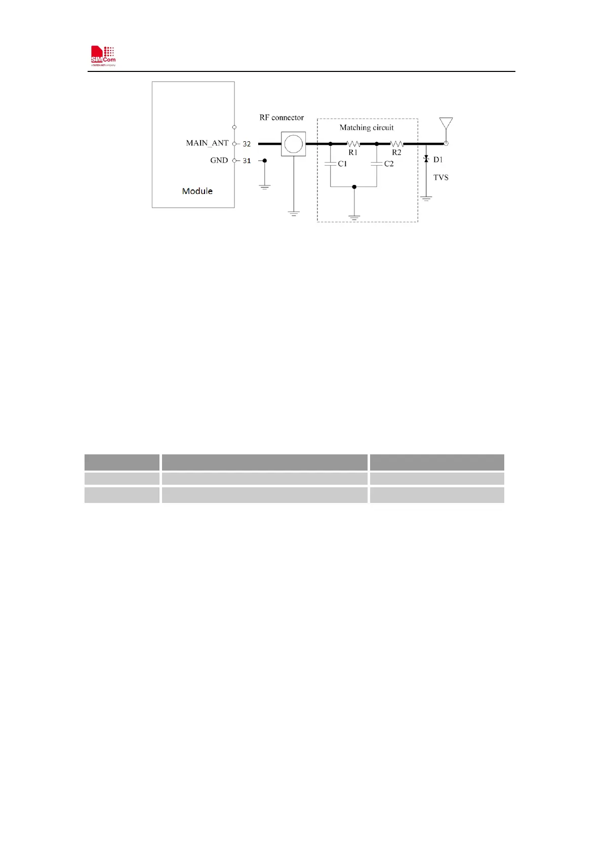
Figure 22: Antenna matching circuit (MAIN_ANT)
In above figure, the components R1,C1,C2 and R2 are used for antenna matching, the values of
components can only be achieved after the antenna tuning and usually provided by antenna vendor.
By default, the R1, R2 are 0Ω resistors, and the C1, C2 are reserved for tuning. The component D1 is
a TVS for ESD protection, and it is optional for users according to application environment.
The RF test connector is used for the conducted RF performance test, and should be placed as close
as to the module’s MAIN_ANT pin. The traces impedance between SIM7000 and antenna must be
controlled in 50Ω.
Two TVS are recommended in the table below.
Table 23: Recommended TVS
Package Part Number Vender
4.3 RF traces note
4.3.1 RF traces layout
Keep the RF trace from module ant pin to antenna as short as possible
RF trace should be 50 Ω either on the top layer or in the inner layer
RF trace should be avoided right angle and sharp angle.
Put enough GND vias around RF traces.
RF trace should be far away from other high speed signal lines.