12
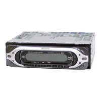
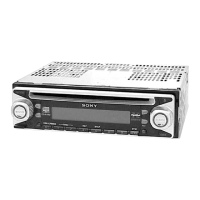
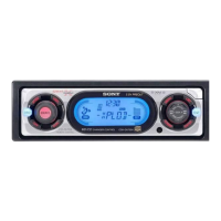
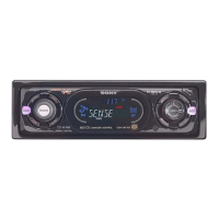
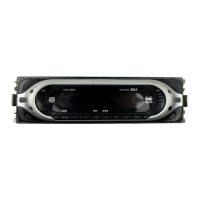
CDX-CA540X/CA590X
3-1. IC PIN DESCRIPTION
• IC801 µPD780076YGK-R24 (SYSTEM CONTROL) (MAIN Board)
Pin No. Pin Name I/O Pin Description
1D SW I Down switch detection signal input “L”: Down switch on
2 LM LD O Loading motor drive control signal output (Loading direction)
3 LM EJ O Loading motor drive control signal output (Eject direction)
4ATT O Mute control signal output of audio signal line “H”: mute on
5A ATTOMute control signal output to power amp IC (IC101) “L”: amp mute on
6 PLL DI I Serial data signal input to PLL IC (IC601)
7VOL ATT O Mute control signal output to Electric volume IC (IC401)
8 DOOR SW/IND I Door switch signal input Case of flipdown, sense to open condition of door “H”: open
9 VSS0 — Ground pin
10 VDD0 — Power supply pin
11 PLL CE O Chip enable signal output to PLL IC (IC601)
12 BEEP O Beep signal output of key beep, caution alarm to power amp IC (IC101)
13 SDAO O IIC data line signal output (control to electric volume IC (IC401))
14 SCLO O IIC clock line signal output (control to electric volume IC (IC401))
15 LCD CE O Chip enable control signal output to LCD driver IC (IC901)
16 LCD DO O Serial data signal output to LCD driver IC (IC901)
17 LCD CLK O Serial clock signal output to LCD driver IC (IC901)
18 BUS SI I SONY bus data signal input from bus interface IC (IC802)
19 BUS SO O SONY bus data signal output to bus interface IC (IC802)
20 BUS CLK I SONY bus clock signal input
21 BUS CLK GEN O SONY bus clock signal output
22 AM ON O
AM select signal output
FM circuit power supply control output of tuner unit (TU601) “H”: FM on
23 FM ON O
FM select signal output
FM circuit power supply control output of tuner unit (TU601) “H”: FM on
24 VDD1 — Power supply pin
25 AVSS — Ground pin
Stereo signal input/monaural control signal output
26 ST IND I/O At forced monaural on: “L” output
At forced monaural off: input mode, stereo on for “L” input
27 SHIFT/PH1 I Rotary commander shift key signal input
28 S METER I S meter signal input from tuner unit (TU601)
29, 30 KEY0, KEY1 I A/D key signal input Input of A/D key matrix and front panel attachment decision.
31 R COM I
Rotary commander AD level signal input
Sense to key voltage level of rotary commander
32 DST SEL I Destination select input from frequency select switch (SW803)
33 TEST I Test mode select signal input “L”: test mode
34 AVREF — Analog reference voltage pin
35 AD ON O LCD INHIBIT signal output
36 RESET I Reset signal input from reset IC (IC902) “H”: reset
37 XT2 — Connect to sub clock (32.768 kHz)
38 XT1 — Connect to sub clock (32.768 kHz)
39 IC — At on board writer: 12 V power supply pin (usually ground pin)
40 X2 — Connect to crystal oscillator (8.38 MHz)
41 X1 — Connect to crystal oscillator (8.38 MHz)
42 VSS1 — Ground pin
43 KEY ACK I Key acknowledge signal input
44 SIRCS I Wireless remote control signal input from remote control receiver IC (IC951)
45 SELF SW I SELF switch detection signal input “L”: SELF switch on
46 BU IN I Backup power supply detection signal input
47 NOSE I Front panel attachment detection signal input from SW801 “L”: panel on
SECTION 3
DIAGRAMS