3
TABLE OF CONTENTS
1. GENERAL
Location of controls................................................................. 4
Connections ............................................................................. 4
2. DISASSEMBLY
2-1. Sub Panel Assy (CD) ........................................................... 6
2-2. CD Mechanism Block ......................................................... 7
2-3. Main Board ......................................................................... 7
2-4. Heat Sink ............................................................................. 8
2-5. Chassis (T) Sub Assy .......................................................... 8
2-6. Lever Section, In Self Sw Board ......................................... 9
2-7. Servo Board......................................................................... 9
2-8. Shaft Roller Assy, Load Sw Board.................................... 10
2-9. Floating Block Assy .......................................................... 10
2-10. Optical Pick-up Block ....................................................... 11
MAIN BOARD CNP701
SERVO BOARD CN1
3. DIAGRAMS
3-1. IC Pin Description............................................................. 12
3-2. Circuit Boards Location .................................................... 14
3-3. Block Diagram –CD Section–........................................... 15
3-4. Block Diagram –Tuner Section– ....................................... 16
3-5. Block Diagram –Display Section– .................................... 17
3-6. Printed Wiring Boards –CD Mechanism Section–............ 18
3-7. Schematic Diagram –CD Mechanism Section– ................ 20
3-8. Printed Wiring Boards –Main Section– ............................ 21
3-9. Schematic Diagram –Main Section (1/2)– ........................ 22
3-10. Schematic Diagram –Main Section (2/2)– ........................ 23
3-11. Printed Wiring Board –Relay Section– ............................. 24
3-12. Printed Wiring Board –Display Section– .......................... 25
3-13. Schematic Diagram –Display Section–............................. 26
3-14. IC Block Diagrams............................................................ 27
4. EXPLODED VIEWS
4-1. Chassis Section ................................................................. 30
4-2. Front panel Section ........................................................... 31
4-3. CD Mechanism Section (1) ............................................... 32
4-4. CD Mechanism Section (2) ............................................... 33
4-5. CD Mechanism Section (3) ............................................... 34
5. ELECTRICAL PARTS LIST ........................................ 35
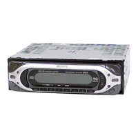
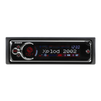
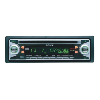
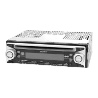
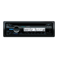
CDX-CA540X/CA590X
EXTENSION CABLE AND SERVICE POSITION
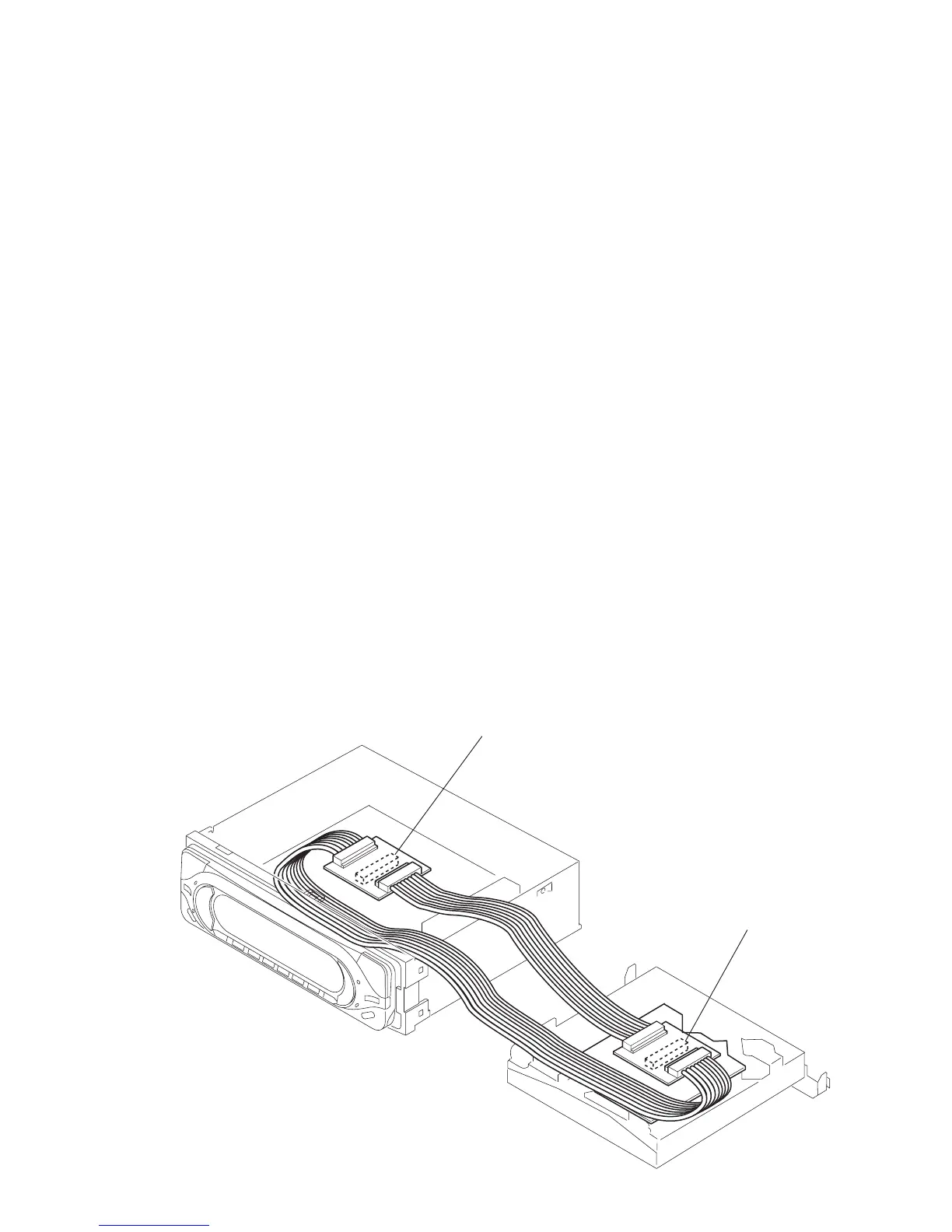
When repairing or servicing this set, connect the jig (extension cable)
as shown below.
• Connect the MAIN board (CNP701) and the SERVO board (CN1)
with the extension cable (Part No. J-2502-062-1).