13
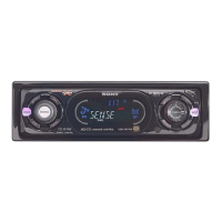
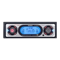
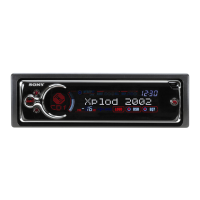
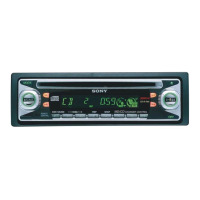
CDX-CA710X/CA790X
3-1. IC PIN DESCRIPTION
• IC303 MN101C49KSD (SYSTEM CONTROL)
Pin No. Pin Name I/O Pin Description
1 VREF– — A/D converter power supply (–) pin
2LVDATA I Spectrum analyzer data input from electronic volume IC.
3 VSM I S-meter voltage detection input
4QUALITY I Noise detection input
5, 6 KEYIN1, 0 I Key input 1, 0
7 RCIN0 I Rotary commander key input
8, 9 NIL I Not used. (Fixed at L in this set)
10 VREF+ — A/D converter power supply (+) pin (+5 V)
11 VDD — Power supply pin (+5 V)
12 OSCOUT O Main clock output (18.43 MHz)
13 OSCIN I Main clock input (18.43 MHz)
14 VSS — Ground
15 XIN I Sub clock input (32.768 kHz)
16 XOUT O Sub clock output (32.768 kHz)
17 MMOD I Memory mode select input (Fixed at L in this set)
18 LCDSO O Serial data output for LCD driver IC.
19 LCDCE O Chip enable output for LCD driver IC.
20 LCDCKO O Serial clock output for LCD driver IC.
21 CD_TSO O Serial data output for CD servo IC.
22 CD_TSI I Serial data input from CD servo IC.
23 CD_TCKO O Serial clock output for CD servo IC.
24 SYSRST O System reset output
25 BUSON O BUS ON output
26 KEYACK I Key acknowledge detection input
27 DAVN I Not used. (Open)
28 BUIN I Backup power supply input
29 SIRCS I SIRCS input
30 TUATTIN I Tuner attenuator control input
31 CD_PACK I CD text pack synchronization signal input from CD servo IC.
32 VDD2 — Power supply pin (+5 V)
33 RESET I Microcomputer reset input
34 NOSESW I Front panel attachment detection input
35 BEEP O Beep output
36 DSTSEL2 I Not used. (Open)
37 TESTIN I Test mode detection input
38 ACCIN I Accessory power supply detection input
39 NCO (VCC) O Not used. (Open)
40 TELATT I Telephone attenuator detection input
41 NCO (VCC) I Not used. (Fixed at H in this set)
42 UNISO O SONY-BUS data output
43 UNISI I SONY-BUS data input
44 UNICKO O SONY-BUS clock output
45 I2C_SIO I/O I
2
C BUS serial data input/output
46 NCO O Not used. (Open)
47 I2C_CKO O I
2
C BUS serial clock output
48 STB O Standby control output for power amp IC.
49 DIAG I Mode input from power amp IC.
50 SELFSW I CD mechanism deck Self switch detection input
SECTION 3
DIAGRAMS