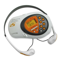
ICF-CD73/CD73V
2121
6-5. NOTE FOR PRINTED WIRING BOARDS AND SCHEMATIC DIAGRAMS
Note on Schematic Diagram:
• All capacitors are in µF unless otherwise noted. pF: µµF
50 WV or less are not indicated except for electrolytics
and tantalums.
• All resistors are in Ω and
1
/
4
W or less unless otherwise
specified.
•
f
: internal component.
• C : panel designation.
• A : B+ Line.
• H : adjustment for repair.
•Power voltage is dc 6 V and fed with regulated dc power
supply from pin 1 and 3 of CNP901 on the JACK board.
•Power voltage is dc 3 V and fed with regulated dc power
supply from pin 2 and 3 of CNP901 on the JACK board.
no mark : FM/TV (2 – 6 ch)
(): AM
[]: TV (7 – 13 ch)/WEATHER (1 – 7 ch)
〈〈 〉〉 : CD PLAY
•Voltages are taken with a VOM (Input impedance 10 MΩ).
Voltage variations may be noted due to normal produc-
tion tolerances.
•Waveforms are taken with a oscilloscope.
Voltage variations may be noted due to normal produc-
tion tolerances.
• Circled numbers refer to waveforms.
• Signal path.
F : FM/TV (2 – 6 ch)
L : TV (7 – 13 ch)/WEATHER (1 – 7 ch)
f : AM
J : CD PLAY
•Abbreviation
CND : Canadian model
IT : Italian model
MX : Mexican model
Note:
The components identi-
fied by mark 0 or dotted
line with mark 0 are criti-
cal for safety.
Replace only with part
number specified.
Note:
Les composants identifiés par
une marque 0 sont critiques
pour la sécurité.
Ne les remplacer que par une
pièce portant le numéro
spécifié.
Note on Printed Wiring Boards:
• X : parts extracted from the component side.
• Y : parts extracted from the conductor side.
• W : indicates side identified with part number.
•
z
: Through hole.
•
f
: internal component.
• : Pattern from the side which enables seeing.
(The other layers' patterns are not indicated.)
Caution:
Pattern face side: Parts on the pattern face side seen from
(Conductor Side) the pattern face are indicated.
Parts face side: Parts on the parts face side seen from
(Component Side) the parts face are indicated.
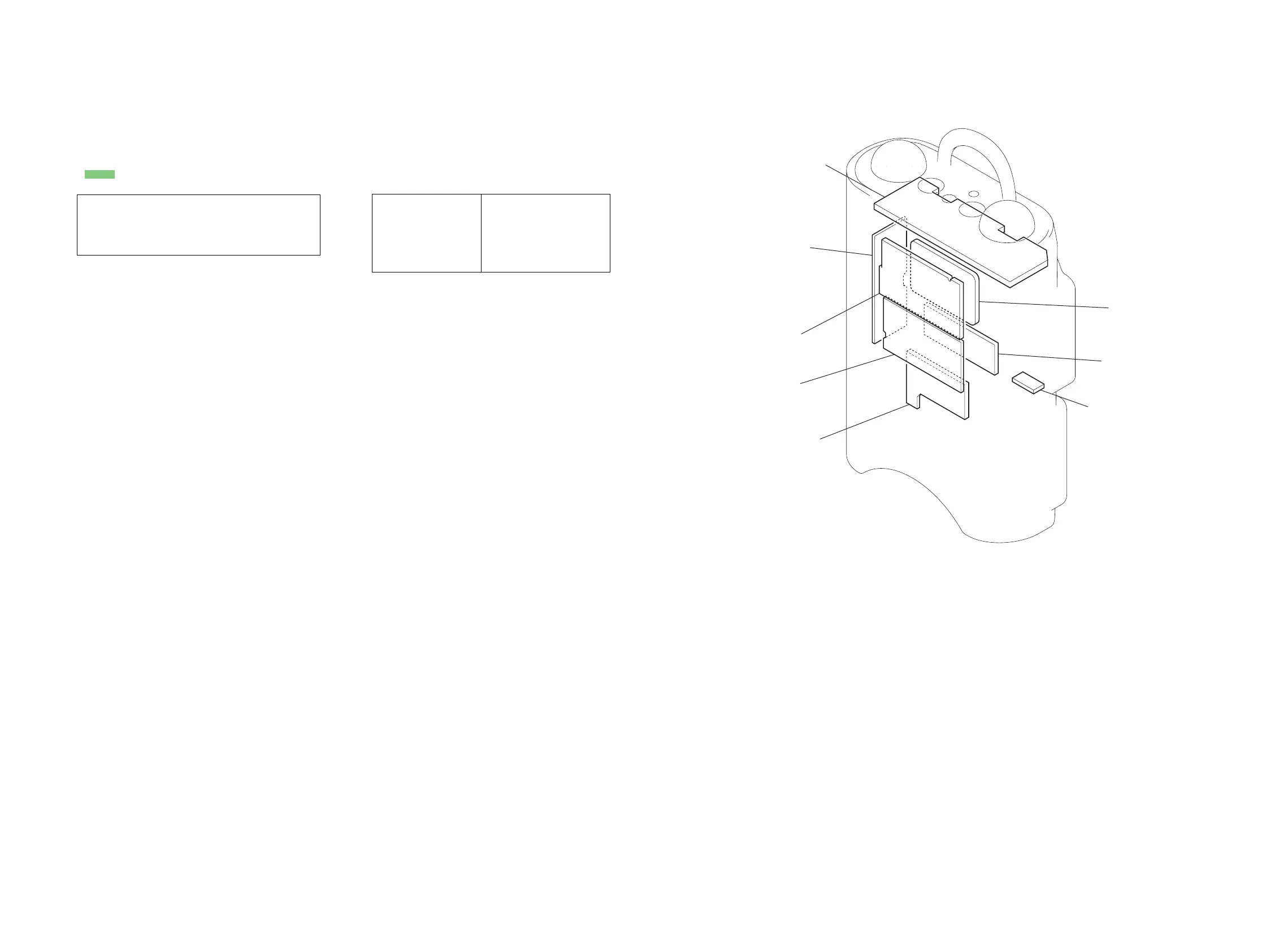
• Circuit Boards Location
LCD board
SW board
tuner board
power board
key board
relay board
jack board
CD boar
Ver. 1.1