3
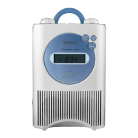
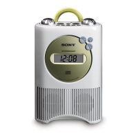
ICF-CD73/CD73V
TABLE OF CONTENTS
1. SERVICING NOTES .............................................. 4
2. GENERAL .................................................................. 5
3. DISASSEMBLY
3-1. Disassembly Flow ........................................................... 6
3-2. Cabinet (Front) Section................................................... 6
3-3. Cabinet (Upper) Section ................................................. 7
3-4. Chassis (Main) Section ................................................... 7
3-5. LCD Board ...................................................................... 8
3-6. Mechanism Deck (KSM-900AAA) ................................ 8
3-7. Optical Pick-up (KSS-900A) .......................................... 9
3-8. Speaker (SP101)/(SP201) ............................................... 9
4. TEST MODE .............................................................. 10
5. ELECTRICAL ADJUSTMENTS........................ 13
6. DIAGRAMS
6-1. Block Diagram – CD Section – .................................... 17
6-2. Block Diagram – TUNER Section (ICF-CD73) – ....... 18
6-3. Block Diagram – TUNER Section (ICF-CD73V) – .... 19
6-4. Block Diagram – MAIN Section – ............................... 20
6-5. Note for Printed Wiring Boards and
Schematic Diagrams ....................................................... 21
6-6. Printed Wiring Board – CD Section – ......................... 22
6-7. Schematic Diagram – CD Section – ............................. 23
6-8. Printed Wiring Board
– TUNER Section (ICF-CD73) – .................................. 24
6-9. Schematic Diagram
– TUNER Section (ICF-CD73) – .................................. 25
6-10. Printed Wiring Board
– TUNER Section (ICF-CD73V) – ............................... 26
6-11. Schematic Diagram
– TUNER Section (ICF-CD73V) – ............................... 27
6-12. Printed Wiring Boards – MAIN Section – ................... 28
6-13. Schematic Diagram – MAIN Section –........................ 29
6-14. Printed Wiring Boards – POWER Section – ................ 30
6-15. Schematic Diagram – POWER Section – .................... 31
6-16. IC Pin Function Description .......................................... 34
7. EXPLODED VIEWS
7-1. Overall Section................................................................ 36
7-2. Cabinet (Front) Section................................................... 37
7-3. Cabinet (Main) Section ................................................... 38
7-4. Cabinet (Upper) Section ................................................. 39
7-5. Cabinet (Rear) Section-1 ................................................ 40
7-6. Cabinet (Rear) Section-2 ................................................ 41
7-7. Cabinet (Rear) Section-3 ................................................ 42
7-8. Optical Pick-up Section (KSM-900AAA) ..................... 43
8. ELECTRICAL PARTS LIST .............................. 44