40
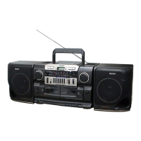
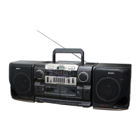
CFD-CD777SMK2
6-16. IC PIN FUNCTION DESCRIPTION
• CONTROL BOARD IC801 CXP5086H-684Q (SYSTEM CONTROLLER, LCD DRIVER)
Pin No. Pin Name I/O Description
1, 2 NC O
Not used
3 SENS I
Internal status input from the DSP
4 SCOR I
Subcode sync (S0+S1) detection signal input from the DSP
5 SQCKO O
Subcode Q data reading clock signal output to the DSP
6, 7 NC O
Not used
8 SQSO I
Subcode Q data input from the DSP
9 CLOK O
Serial data transfer clock signal output to the DSP
10 XLAT O
Serial data latch pulse signal output to the DSP
11 DATA O
Serial data output to the DSP
12 XRST O
Reset signal output to the RF AMP, DSP and D/A converter “L”: reset
13 GND —
Ground terminal
14 REC I
REC/PB switch input terminal “L”: recording mode
15 DOOR I
CD lid open/close detection switch input terminal “L”: CD lid is closed
16 TEST I
Setting terminal for the service mode “L”: service mode, Normally: fixed at “H”
17 NC O
Not used
18 LCD I
Fixed at “L” in this set
19 MODE
I PLAY MODE key input terminal “L” is input when the key pressing
20 DISP
I DISPLAY/ENTER key input terminal “L” is input when the key pressing
21 K-PLAY
I Play/pause (N X) key input terminal “L” is input when the key pressing
22 K-STOP
I Stop (x) key input terminal “L” is input when the key pressing
23 K-FR
I Fast rewind (>) key input terminal “L” is input when the key pressing
24 K-FF
I Fast forward (.) key input terminal “L” is input when the key pressing
25 GND —
Ground terminal
26 VDD —
Power supply terminal (+5V)
27 NC O
Not used
28 C-MUTE O
Muting control signal output to the DSP, D/A converter and line muting circuit “H”: muting on
29 to 33 NC O
Not used
34 LDON O
Laser diode on/off control signal output terminal “H”: laser on
35 NC O
Not used
36 SEG14 O
Segment drive signal output terminal Not used
37 to 50 SEG13 to SEG0 O
Segment drive signal output to the liquid crystal display
51 to 54 COM3 to COM0 O
Common drive signal output to the liquid crystal display
55 VLC1 I
Power supply input for the liquid crystal display
56 VLC2 I
Power supply input for the liquid crystal display
57 VLC3 I
Power supply input for the liquid crystal display
58 VDD —
Power supply terminal (+5V)
59 VL I
Power supply input for the liquid crystal display
60 XTAL O
Main system clock output terminal (4.019 MHz)
61 EXTAL I
Main system clock input terminal (4.019 MHz)
62 RST O
Reset signal output to the motor/coil driver IC “L”: reset
63 GND —
Ground terminal
64 RMC-S I
Sircs remote control signal input from the remote control receiver