39
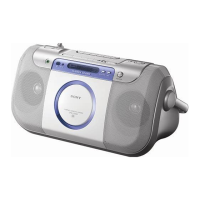
CFD-E77L
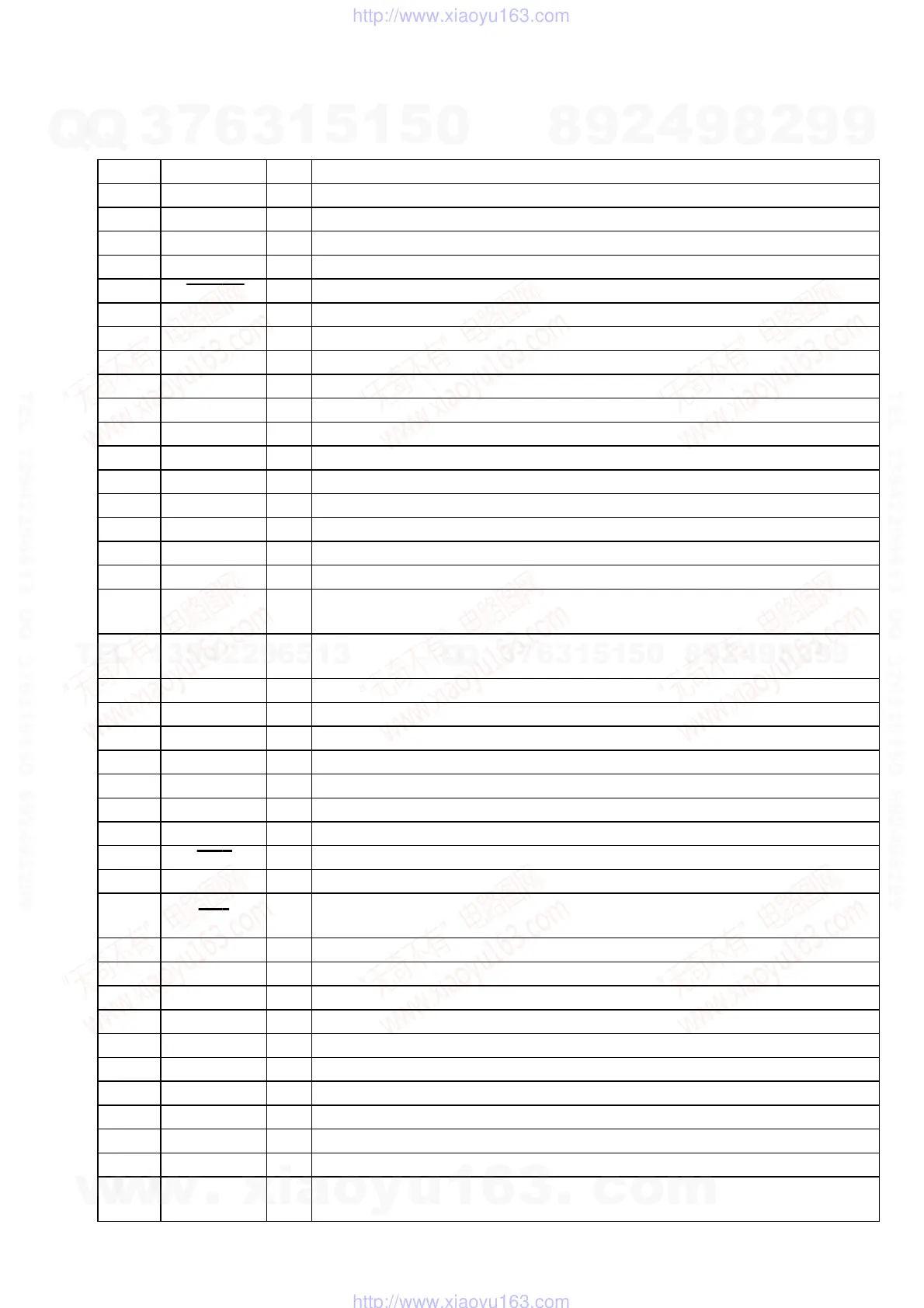
• MAIN BOARD IC801 CXP83624-035Q (SYSTEM CONTROLLER)
Pin No. Pin Name
I/O
Description
1 CD-WRQ I Interruption detection signal input from the digital signal processor
2 RMC I Sircs remote control signal input
3 BUZZER O Buzzer sound signal output
4 N.C O Not used
5 CD-RES O System reset signal output to the digital signal processor “L”: reset
6 CD CE O Chip enable signal output to the digital signal processor
7 CD CL O Serial data transfer clock signal output to the digital signal processor
8 CD DO I Serial data input from the digital signal processor
9 CD DI O Serial data output to the digital signal processor
10 CD DRF I Focus on/off detection signal input from the digital signal processor
11 CD FSEQ I Synchronizing signal detection signal input from the digital signal processor
12 V-DATA O
Serial data output to the electrical volume
13 V-CLOCK O
Serial data transfer clock signal output to the electrical volume
14 N.C O Not used
15 MEGABASS O Megabass on/off control signal output “L”: megabass on
16 A-MUTE O Audio muting on/off control signal output to the electrical volume “H”: muting on
17 N.C O Not used
18
CD
O
Power on/off control signal output for the CD +5V power supply, and CD function control signal
output to the recording/playback equalizer amplifier “H”: CD power on
19 P-CON O
Power on/off control signal output to the power supply circuit, and power amplifier
“L”: standby mode, “H”: power on
20 CD DOOR I
CD lid open/close detection switch input terminal “L”: CD lid is closed, “H”: CD lid is opened
21 REG CHK I Regulator check signal input of the AC input or battery input “H” active
22
N.C O Not used
23, 24 KEY-1, KEY-2 I Key input terminal (A/D input)
25 JOG-B I Jog dial pulse input from the rotary encoder (B phase input)
26 JOG-A I Jog dial pulse input from the rotary encoder (A phase input)
27
SIMUKE CHECK
I Destination setting terminal
28 INIT O Initial setting signal output
29 SHIFT CLK O Shift clock output of the main system clock (4.19 MHz) “H” active
30 RST I
System reset signal input “L”: reset
For several hundreds msec. after the power supply rises, “L” is input, then it changes to “H”
31 EXTAL I Main system clock input terminal (4.19 MHz)
32 XTAL O Main system clock output terminal (4.19 MHz)
33 VSS — Ground terminal
34 VL O Liquid crystal display drive bias control signal output terminal
35 to 37 VLC3 to VLC1 — Terminal for doubler circuit capacitor connection to develop liquid crystal display drive voltage
38 to 41 COM0 to COM3 O
Common drive signal output to the liquid crystal display
42 to 61 SEG0 to SEG19 O
Segment drive signal output to the liquid crystal display
62 to 64 N.C O Not used
65 RADIO O
Power on/off control signal output for the radio +6V power supply “H”: radio power on
66 TU-CE O PLL chip enable signal output to the FM/AM PLL
67 TAPE O
Tape function control signal output to the recording/playback equalizer amplifier
“L”: radio or CD on, “H”: tape on
6-19. IC PIN FUNCTION DESCRIPTION
w
w
w
.
x
i
a
o
y
u
1
6
3
.
c
o
m
Q
Q
3
7
6
3
1
5
1
5
0
9
9
2
8
9
4
2
9
8
T
E
L
1
3
9
4
2
2
9
6
5
1
3
9
9
2
8
9
4
2
9
8
0
5
1
5
1
3
6
7
3
Q
Q
TEL 13942296513 QQ 376315150 892498299
TEL 13942296513 QQ 376315150 892498299
http://www.xiaoyu163.com
http://www.xiaoyu163.com