44
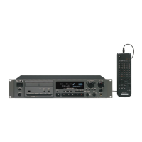
CFD-RS60CP
46 AoUT3 (PO4) O Request signal output to the USB controller Not used. (Open)
47 AoUT2 (PO5) O Audio data output to the USB controller
48 PIO0 O Request signal output to the system controller or USB controller
49 PIO1 O ST REQ signal output
50 PIO2 O Not used. (Open)
51 PIO3 I Gate signal input from the USB controller
52 VSS1 — Ground
53 VDDT3 — Power supply (+3.3 V)
54 SBSY O Subcode block sync signal output to the system controller
55 SBOK/FOK O Not used. (Open)
56 IPF O Not used. (Open)
57 SFSY/LOCK O Not used. (Open)
58 ZDET O Zero detection signal output Not used. (Open)
59 GPIN I Not used. (Connected to ground.)
60 MS I Microcomputer interface mode selection signal input Fixed at “H” in this set.
61 DOUT (PO6) O Digital audio data output Not used in this set. (Open)
62 AOUT1 (PO7) O Audio data output Not used in this set. (Open)
63 BCK (PO8) O Bit clock signal output to the USB controller
64 LRCK (PO9) O L/R sampling clock signal output
65 AIN (PI4) I Digital audio data input from the USB controller
66 BCKi (PI5) I Bit clock signal input from the USB controller
67 LRCKi (PI6) I L/R sampling clock signal input from the USB controller
68 VDD1 — Power supply (+1.5 V)
69 VSS — Ground
70 AWRC — Not used. (Open)
71 PVDD3 — Power supply (+3.3 V)
72 PDO O Phase error margin signal between EFM signal and PLCK signal output
73 TMAXS O TMAX detection signal output Not used. (Open)
74 TMAX O TMAX detection signal output
75 LPFN I Inverted signal input from the operation amplifier for PLL loop filter
76 LPFo O Signal output from the operation amplifier for PLL loop filter
77 PVREF I Reference voltage (+1.65 V) input
78 VCOF O VCO filter output
79 PVSS3 — Ground
80 SLCo O EFM slice level output
81 RFi I RF signal input
82 RFRPi I RF ripple signal input
83 RFEQo O EFM slice level output
84 VRo O Reference voltage (+1.65 V) output
85 RESiN O External resistor connection pin
86 VMDiR O Reference voltage (+1.65 V) output for automatic power control circuit
87 TESTR O Low-pass filter terminal for RFEQO offset correction
88 AGCi I RF signal amplitude adjustment amplification input
89 RFo O RF signal generation amplification output
90 RVDD3 — Power supply (+3.3 V)
91 LDo O
Laser diode on/off control signal output to the automatic power control circuit
“H”: laser diode on
Pin No. Pin Name I/O Pin Description
 Loading...