46
CFD-RS60CP
IC801 MB90F045PF-G-9055-SPE1 (SYSTEM CONTROL) (MAIN BOARD (1/2))
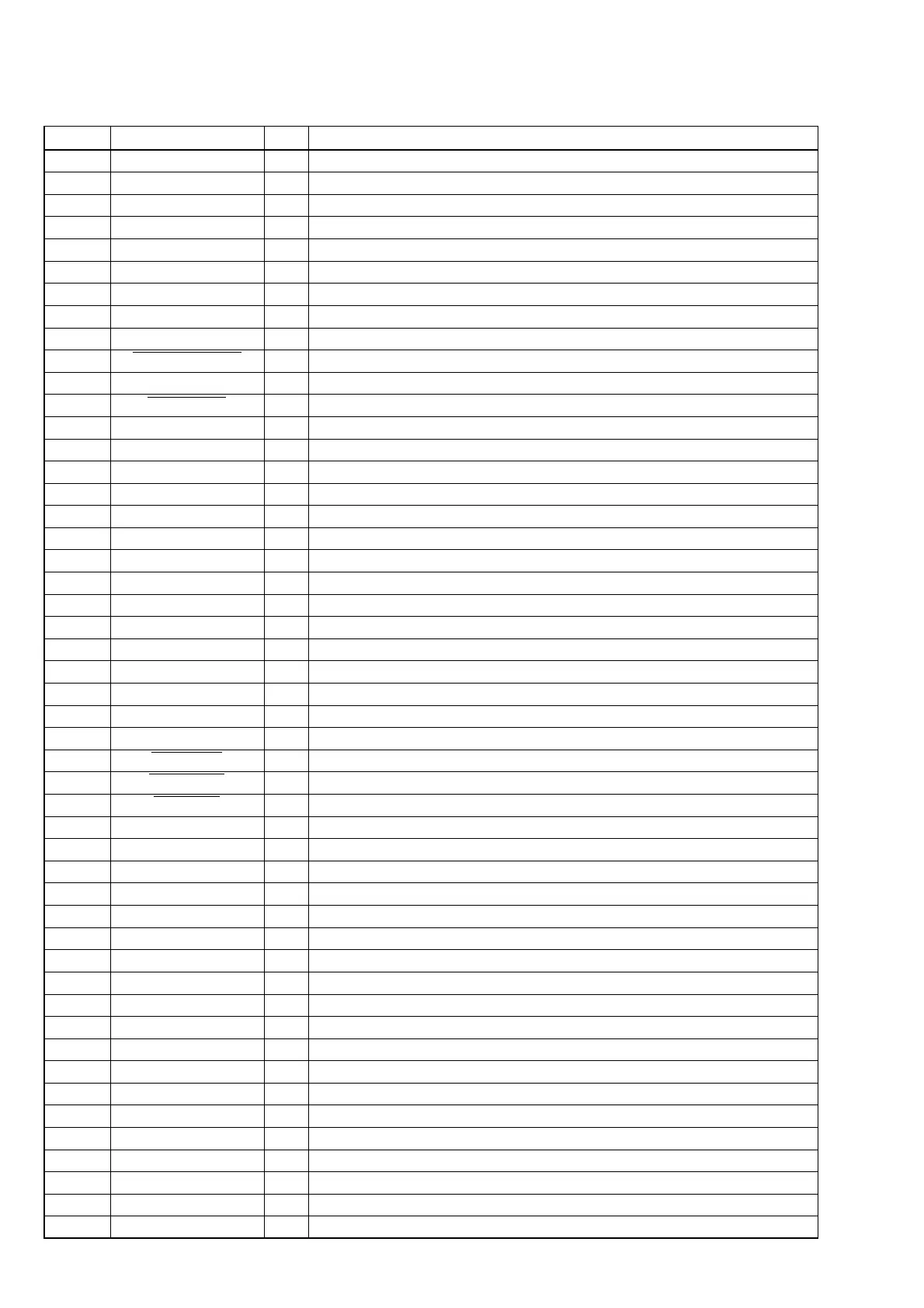
Pin No. Pin Name I/O Pin Description
1 I-SIMUKE1 I Destination setting pin
2 I-SIMUKE2 I Destination setting pin
3 I-SIMUKE3 I Destination setting pin
4 to 6 NC — Not used. (Open)
7 Z-BUS0 I/O Serial bus data bit 0 input/output
8 Z-BUS1 I/O Serial bus data bit 1 input/output
9 Z-BUS2 I/O Serial bus data bit 2 input/output
10 Z-BUS3 I/O Serial bus data bit 3 input/output
11 VSS — Ground
12 O-DEC-BUS-SEL O Bus control switch signal output “H”:USB, “L”:CD
13 O-TU-ON O Tuner on/off signal output
14 O-TU-MUTE O Tuner mute control signal output
15 I-TU-COUNT I Tuner PLL IF count input
16 O-TU-CLK O Tuner PLL clock signal output
17 O-TU-DATA O Tuner PLL data signal output
18 O-TU-CE O Tuner PLL chip enable signal output
19 O-LCD-SI O LCD driver control serial data output
20 O-LCD-SCK O LCD driver control serial clock output
21 NC — Not used. (Open)
22 NC — Not used. (Open)
23 VGGS — Power supply (+3.3V)
24 O-USB-CTS I Clear to send signal input from USB controller
25 I-USB-RTS O Ready to send signal output to USB controller
26 O-USB-RST O Reset signal output to the USB controller
27 USB-RXD(SI) I Serial data input from the USB controller
28 USB-TXD(SO) O Serial data output to the USB controller
29 NC(SC) — Not used. (Open)
30 O-LCD-INH O LCD drive inhibit signal output
31 O-LCD-RST O LCD drive reset signal output
32 O-LCD-CS O LCD drive chip select signal output
33 EPROM-SCL O EPROM serial clock signal output
34 EPROM-SDA I/O EPROM serial data signal input/output
35 AVCC — A/D converter power supply (+3.3V)
36 AVRH — A/D converter external reference voltage supply
37 AVSS — A/D converter Ground
38 I-KEY0 I Key signal input 0
39 I-KEY1 I Key signal input 1
40 I-KEY2 I Key signal input 2
41 I-KEY3 I Key signal input 3
42 VSS — Ground
43 I-REG3.3V-CHK I REG 3.3V on/off check input
44 I-REG6.0V-CHK I Electric volume power supply voltage check input
45 I-VH(REG9.0V-CHK) I Battery voltage check input
46 I-VM I Battery VM voltage check input
47 I-WAKE UP(INT0) I Key wake up trigger signal input
48 (INT1) — Not used. (Open)
49 (MD0) I Operation mode setting pin (Pull up)
50 (MD1) I Operation mode setting pin (Pull up)
51 (MD2) I Operation mode setting pin (Pull down)


 To Next Page