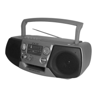
CFD-V27
— 15 — — 16 — — 17 — — 18 —
R
DISPLAY/ENTER
PLAY MODE
2-4. SCHEMATIC DIAGRAM MAIN SECTION • Refer to page 7 for Printed Wiring Board. • Refer to page 22 for IC Block Diagrams.
• Waveforms
2
IC701 #£ RFO
3
IC702 ` XTAO
0.2V/div
0.5µsec/div
2V/div
50µsec/div
104
5 Vp-p
1.0 Vp-p
16.9 MHz
Note on Schematic Diagram:
• All capacitors are in µF unless otherwise noted. pF: µµF
50 WV or less are not indicated except for electrolytics
and tantalums.
• All resistors are in Ω and
1
/
4
W or less unless otherwise
specified.
•
¢
: internal component.
• U : B+ Line.
• H : adjustment for repair.
• Power voltage is dc 3V and fed with regulated dc power
supply from external power voltage jack (J301) .
• Voltages and waveforms are dc with respect to ground
under no-signal (detuned) conditions.
[ ] : FM
< > : PB
• Voltages are taken with a VOM (Input impedance 10 MΩ).
Voltage variations may be noted due to normal produc-
tion tolerances.
• Waveforms are taken with a oscilloscope.
• Signal path.
F : FM
f : AM
E : PB
a : REC
J : CD
The components identified by mark 0 or dotted
line with mark 0 are critical for safety.
Replace only with part number specified.