– 19 – – 20 –
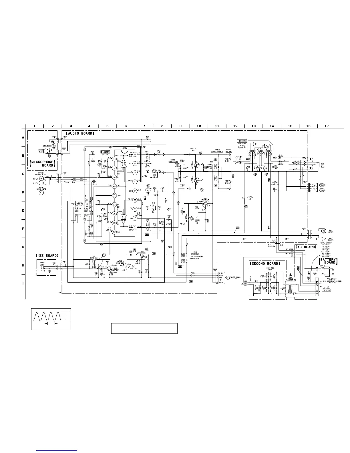
5-6. SCHEMATIC DIAGRAM — MAIN SECTION —
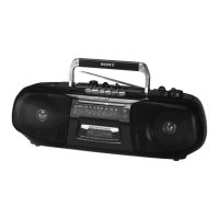
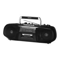
CFS-B5LMK2
Note:
• All capacitors are in µF unless otherwise noted. pF: µµF
50 WV or less are not indicated except for electrolytics
and tantalums.
• C : panel designation.
Note: The components identified by mark ! or dotted line
with mark ! are critical for safety.
Replace only with part number specified.
• U : B+ Line.
• Total current is measured with no cassette installed.
• Power voltage is dc 9 V and fed with regulated dc power
supply from battery terminal.
• Voltage and waveforms are dc with respect to ground
under no-signal (detuned) conditions.
no mark : FM
< > : PB
<< >> : REC
• Voltages are taken with a VOM (Input impedance 10 MΩ).
Voltage variations may be noted due to normal produc-
tion tolerances.
• Waveforms are taken with a oscilloscope.
Voltage variations may be noted due to normal produc-
tion tolerances.
• Circled numbers refer to waveforms.
• Signal path.
F : FM
E : PB
a : REC
(Page 16)
T301
• Waveform (MODE:REC)
1
35Vp-p
15mS