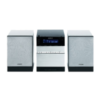
HCD-DC1
1818
6-4. NOTE FOR PRINTED WIRING BOARDS AND SCHEMATIC DIAGRAMS
Note on Printed Wiring Boards:
• X : parts extracted from the component side.
• Y : parts extracted from the conductor side.
• W : indicates side identified with part number.
• : Pattern from the side which enables seeing.
• Indication of transistor.
Note on Schematic Diagram:
• All capacitors are in µF unless otherwise noted. pF: µµF
50 WV or less are not indicated except for electrolytics
and tantalums.
• All resistors are in Ω and
1
/
4
W or less unless otherwise
specified.
•
f
: internal component.
• C : panel designation.
• A : B+ Line.
• B : B– Line.
• H : adjustment for repair.
• Voltages are taken with a VOM (Input impedance 10 MΩ).
Voltage variations may be noted due to normal produc-
tion tolerances.
• Waveforms are taken with a oscilloscope.
Voltage variations may be noted due to normal produc-
tion tolerances.
• Circled numbers refer to waveforms.
• Signal path.
F : TUNER
E : TAPE PLAY (DECK A)
d : TAPE PLAY (DECK B)
G : TAPE REC
J : CD PLAY (ANALOG)
c : CD PLAY (DIGITAL)
• Abbreviation
CND : Canadian model
HK : Hong Kong model
MX : Mexican model
MY : Malaysia model
SP : Singapore model
Note: The components identified by mark 0 or dotted line
with mark 0 are critical for safety.
Replace only with part number specified.
C
B
These are omitted.
E
Q
B
These are omitted.
CE
Q
B
These are omitted.
CE
Q
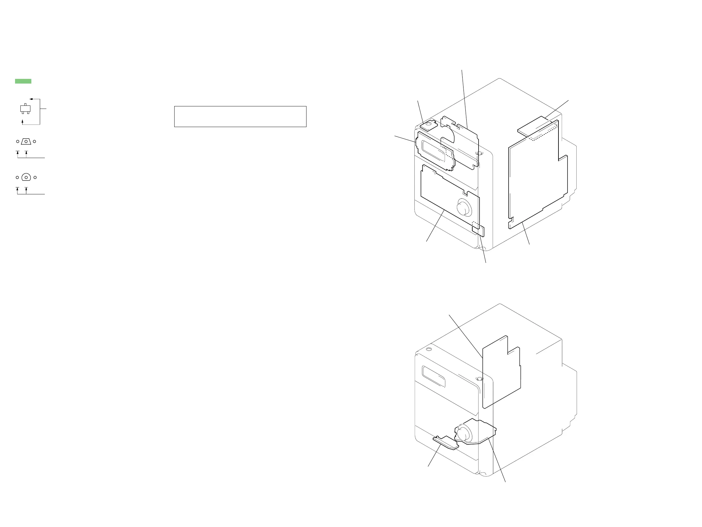
• Circuit Boards Location
TC board
LCD board
I/O SWITCH board
SWITCH board
HEADPHONE board
MAIN board
TUNER UNI
• Abbreviation
CND : Canadian model
HK : Hong Kong model
MX : Mexican model
MY : Malaysia model
SP : Singapore model
Ver 1.1
POWER board
CD board
LOADING board
 Loading...