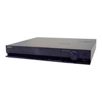
HBD-DZ170/DZ171/DZ175/DZ310/DZ510/DZ610/DZ810
64
Pin No. Pin Name I/O Description
63, 64 HA18, HA19 O Flash ROM address bus A18, A19 output
65 DVDD3 — Power supply (+3.3V)
66 XWR O Flash ROM write signal output
67 to 74 HA16 to HA9 O Flash ROM address bus A16 to A9 output
75 HA20 Flash ROM address bus A20 output
76 XROMCS O Flash ROM chip select signal output
77 HA1 O Flash ROM address bus A1 output
78 XRD O Flash ROM read signal output
79, 80 HD0, HD1 I/O Flash ROM data bus D0, D1 input/output
81 DVSS — Ground terminal
82 to 86 HD2 to HD6 I/O Flash ROM data bus D2 to D6 input/output
87 HA21 I/O Flash ROM data bus D21 input/output
88 RESERVED — Not used. (Open)
89 HD7 I/O Flash ROM data bus D7 input/output
90 DVSS — Ground terminal
91, 92 HA17, HA0 O Flash ROM address bus A17, A0 output
93 DVDD18 — Power supply (+1.8V)
94 FWD O Tray loading motor control (FWR) signal output
95 REV O Tray loading motor control (REV) signal output
96 DVDD3 — Power supply (+3.3V)
97 IFSDO O CPU I/F serial data output
98 IFCK O CPU I/F serial clock output
99 xIFCS O CPU I/F chip select output
100 IFSDI I CPU I/F serial data input
101 SCL O EEPROM serial clock output
102 SDA I/O EEPROM serial data input/output
103 CKSW I Chuck/Tray detect switch signal input
104 OCSW I Chuck/Tray detect switch signal input
105 RXD I RXD signal input from Jig
106 TXD O TXD signal output to Jig
107 ICE O Not used. (Open)
108 xSYSRST I System reset signal input
109 RESERVED I Not used. (Open)
110 xIFBSY I Busy signal input from CPU I/F
111 DQM0 O SDRAM lower byte mask enable signal output
112 EEWP O EEPROM ready/Busy wake up signal output
113 to 117 RD7 to RD3 I/O SDROM data bus D7 to D3 input/output
118 DVDD3 — Power supply (+3.3V)
119 to 121 RD2 to RD0 I/O SDROM data bus D2 to D0 input/output
122 to 129 RD15 to RD8 I/O SDROM data bus D15 to D8 input/output
130 TSD_M I TSD signal input
131 DVDD3 — Power supply (+3.3V)
132 DQM1 O SDRAM upper byte mask enable signal output
133 _RWE O SDRAM write enable signal output
134 _CAS O SDRAM column address strobe signal output
135 _RAS O SDRAM row address strobe signal output
136 _RCS O SDRAM chip select signal output
137, 138 BA0, BA1 O SDRAM bank address 0, 1 output
139 RA10 O SDRAM address bus A10 output
140, 141 RA0, RA1 O SDRAM address bus A0, A1 output
142 DVDD18 — Power supply (+1.8V)
143, 144 RA2, RA3 O SDRAM address bus A0, A3 output
145 DVDD3 — Power supply (+3.3V)
146 DRCLK O SDRAM clock output
147 CKE O SDRAM clock enable signal output
148 DVSS — Ground
149 RA11 O SDRAM address bus A11 output
150 to 155 RA9 to RA4 O SDRAM address bus A9 to A4 output
156 DVDD3 — Power supply (+3.3V)