51
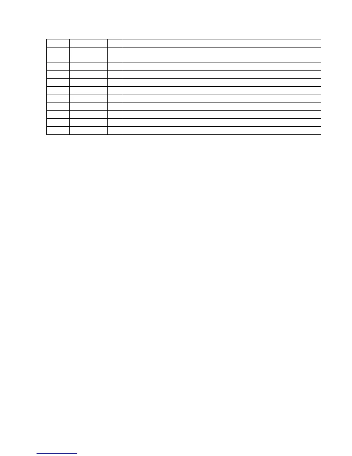
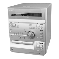
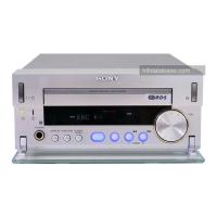
HCD-BX5BT/CBX1/CBX3
Pin No.
Pin Name
I/O
Description
91
LDo O
Laser diode on/off control signal output to the automatic power control circuit
"H": laser diode on
92
MDi
I
Light amount monitor input from the laser diode of optical pick-up block
93
RVSS3 - Ground terminal
94
FNi2 (C)
I
Main beam (C) input from the optical pick-up block
95
FNi1 (A)
I
Main beam (A) input from the optical pick-up block
96
FPi2 (D)
I
Main beam (D) input from the optical pick-up block
97
FPi1 (B)
I
Main beam (B) input from the optical pick-up block
98
TPi (F)
I
Sub beam (F) input from the optical pick-up block
99
TNPC O External capacitor connection terminal
100
TNi (E)
I
Sub beam (E) input from the optical pick-up block