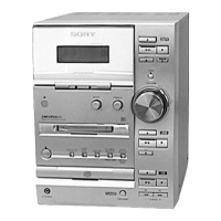
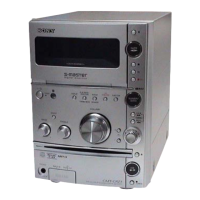
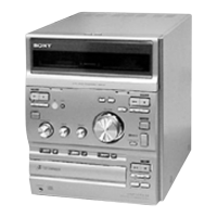
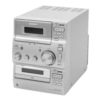
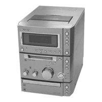
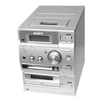
HCD-CPX22/NXM3
2121
HCD-CPX22/NXM3
•WAVEFORMS
– MAIN BOARD –
IC401 0 XC-IN
VOL/DIV : 0.5 V AC
TIME/DIV : 2.0
µ
sec
2
IC401 qg X-IN
VOL/DIV : 0.5 V AC
TIME/DIV : 50 nsec
2
IC703 6
VOL/DIV : 1 V AC
TIME/DIV : 50 nsec
1
1.5Vp-p
32.768KHz
1.5Vp-p
16MHz
2Vp-p
12.288 MHz
– BD BOARD –
IC101 wa TEI
VOL/DIV : 0.2 V AC
TIME/DIV : 0.2 msec
2
IC101 wd FEI
VOL/DIV : 0.1 V AC
TIME/DIV : 1 msec
3
IC101 ra RFACO
VOL/DIV : 0.2 V AC
TIME/DIV : 0.5
µ
sec
1
– S-MASTER BOARD –
IC705 rk XFSOIN
VOL/DIV : 2 V AC
TIME/DIV : 20 nsec
1
0.15Vp-p
0.4Vp-
0.96Vp-p
SECTION 7
DIAGRAMS
For schematic diagrams.
Note:
• All capacitors are in µF unless otherwise noted. (p: pF)
50 WV or less are not indicated except for electrolytics
and tantalums.
• All resistors are in Ω and
1
/
4
W or less unless otherwise
specified.
•%: indicates tolerance.
• f : internal component.
• 2 : nonflammable resistor.
• 5 : fusible resistor.
• C : panel designation.
• A : B+ Line.
• B : B– Line.
• H : adjustment for repair.
•Voltages and waveforms are dc with respect to ground
under no-signal conditions.
no mark: TUNER (FM/AM)
( ): CD PLAY
< >: TAPE PLAY
[ ]: TAPE REC
* : Impossible to measure
•Voltages are taken with a VOM (Input impedance 10 MΩ).
Voltage variations may be noted due to normal produc-
tion tolerances.
•Waveforms are taken with a oscilloscope.
Voltage variations may be noted due to normal produc-
tion tolerances.
• Signal path.
F : TUNER (FM/AM)
E : TAPE PLAY (DECK A)
d : TAPE PLAY (DECK B)
G : RECORD
J : CD PLAY (ANALOG OUT)
c : CD PLAY (DIGITAL OUT)
• Abbreviation
E3 : 240V AC Area in E model
E51 : Chilean and Peruvian model
EA : Saudi Arabia mdoel
RU : Russian model
Note: The components identified by mark 0 or dotted line
with mark ! are critical for safety.
Replace only with part number specified.
(The other layers' patterns are not indicated.)
• Indication of transistor.
• Abbreviation
E3 : 240V AC Area in E model
E51 : Chilean and Peruvian model
EA : Saudi Arabia mdoel
RU : Russian model
Caution:
Parts face side: Parts on the parts face side seen from
(Side A) the parts face are indicated.
Pattern face side: Parts on the pattern face side seen from
(Side B) the pattern face are indicated.
C
B
These are omitted.
E
Q
B
These are omitted.
CE
Q
B
These are omitted.
CE
Q
Note on Printed Wiring Boards:
Note:
• X : parts extracted from the component side.
•
: Pattern from the side which enables seeing.
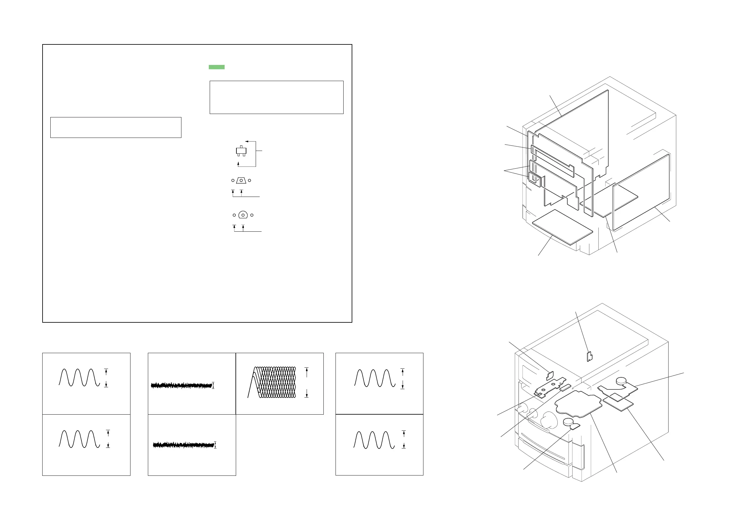
7-1. CIRCUIT BOARD LOCATION
MAIN board
PANEL board
DISC SW board
VOL board
HP board
S-MASTER board
switching regulator
SW(2) board
SW(1) board
MOTOR board
SENSOR board
ENCODER board
BD board
RELAY board
SP OUT board