41
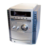
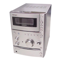
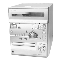
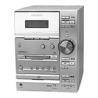
HCD-CPX22/NXM3
7-21. IC Pin Function Descriptions
• IC101 CXD3059AR (RF AMP) (BD BOARD)
Pin No. Pin Name I/O Description
1MIRR I/O Mirror signal input/output(Not used)
2 DFCT I/O Defect signal input/output (Not used)
3 FOK I/O Focus OK signal input/output (Not used)
4 VSS — Internal digital ground
5 LOCK I/O Not used
6 MDP O Spindle motor servo control output
7 SSTP I Disk innermost detection signal input
8 IOVSS1 — I/O digital ground
9 SFDR O Sled drive output
10 SFDR O Sled drive output
11 TFDR O Tracking drive output
12 TRDR O Tracking drive output
13 FFDR O Focus drive output
14 FFDR O Focus drive output
15 IOVDD1 — I/O digital power supply
16 AVDD0 — Analog power supply
17 AVSS0 — Analog ground
18 NC — Not used
19 E I E signal input
20 F I F signal input
21 TEI I Tracking error signal input
22 TEO O Tracking error signal output
23 FEI I Focus error signal input
24 FEO O Focus error signal output
25 VC I/O Center voltage output from RF amplifier block
26 A I A signal input
27 B I B signal input
28 C I C signal input
29 D I D signal input A
30 NC — Not used
31 AVDD4 — Analog power supply
32 RFDCO O RFDC signal output (Not used)
33 PDSENS I Reference voltage pin
34 AC_SUM O RFAC summing amplifier output
35 EQ_IN I Equalizer circuit input
36 LD O APC output
37 PD I APC input
38 NC — Not used
39 RFC I Equalizer cut-off frequency adjustment pin
40 AVSS4 — Analog ground
41 RFACO O RFAC signal output
42 RFACI I RFAC signal input or EFM signal input
43 AVDD3 — Analog power supply
44 BIAS I Asymmetry circuit constant current input
45 ASYI I Asymmetry comparator voltage input
46 ASYO O EFM full-swing output
47 VPCO O Not used
48 VCTL I Wide-band EFM PLL VCO2 control voltage input